What’s the Difference Between DC-DC Conversion Topologies?

Power supplies represent the conversation topic for every circuit designer across the landscape of electrical designs. For instance, you can delve into sensor, Internet of Things (IoT), automation, transportation, medical, or fitness circuit solutions and in every case, one of the primary challenges is to design an appropriate power-supply network for your circuit.
Power-supply classifications come in many flavors. At the top level are the basic ac-ac, ac-dc, dc-ac, or dc-dc converters. In this article, we’ll discuss the dc-dc conversion category in terms of shifting the power signal down with a low-dropout regulator (LDO) or buck topologies, and up with a boost topology.
Low-Dropout Regulator
When designing your power-supply circuit with an LDO, you’re embarking on a simple, straightforward and inexpensive way to change your higher dc voltage down to a smaller voltage.
A linear regulator, or LDO, uses a voltage-controlled current source (VCCS) or transistor to force the regulator’s output to a fixed voltage. The control circuitry continuously senses the output voltage and adjusts the current source to hold the output voltage to the predetermined value. The pass transistor’s current determines the maximum regulator output-current load while maintaining regulation (Fig. 1).
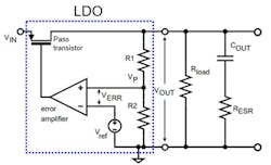
1. The basic LDO circuit design has a pass transistor to provide variable output currents and the topology, though VREF, the error amplifier, and R1/R2 is pre-programmed to provide a relative stable output voltage.
In Fig. 1, the LDO elements are the pass transistor, error amplifier, voltage reference (Vref), and the feedback/gain resistors (R1 and R2). The Vref and R1+R2 establish the regulator’s output dc voltage. A key element in this circuit is the pass transistor. The error-amplifier feedback loop and the voltage reference controls the pass transistor’s gate and thereby influences the amount of current that goes to Rload. This transistor acts like an adjustable current source and responds to varying changes with the output load.
To assure loop stability, this feedback loop requires loop stability compensation. You will find that most LDOs have built-in compensation to ensure stability without added external components.
The output capacitor parasitic resistance, RESR, produces a zero into the LDO feedback system. The frequency of this zero is equal to:
fZERO = 1/(2 × π × RESR × COUT)
This zero will add a phase shift to the compensation loop. Typically, manufacturer’s datasheets address this issue and provide ample guidance.
The LDO is a linear device that theoretically produces a linear power supply, but don’t be fooled into using this device in your system and assume you have a good low-noise power supply. These devices will produce a relatively low-noise output voltage with an efficiency of VOUT/VIN; however, their power-supply-rejection capability may not rise to the task of eliminating input noise.
For example, you can have a switching power supply provide the input voltage to your LDO. If the switching power supply’s frequency is high enough, that switching noise may pass right through the LDO and to the output pin.
Switched-Mode Power Supply (SMPS)
The LDO is strictly a linear device that doesn’t have any involvement with clock signals, which is contrary to the rest of the devices discussed in this article. In their most-basic form, the currents in the switching regulator require incremental breaks in the current source followed by a filter to reconstitute the dc signal to the output. The non-synchronous buck, synchronized buck, and boost power converters accomplish this with five devices: switch, inductor, capacitor, diode, and clock.
The classes in this technology are the switching regulator and switching controller. These devices are very similar. The configuration for both are dc-dc converters and can generally be either buck or boost.
The switching regulator’s integrated circuit (IC) contains all of the necessary components except for the inductor, and a few resistors and capacitors. It’s important to notice that the switching regulator’s IC chip includes the FET switch. As a result, switching regulators can’t handle too much current. Usually the maximum output current is 1 to 2 A.
In contrast, the switching controller’s IC has the same components as the switching regulator, with one exception. The switching regulator doesn’t have the FET switch within the IC; it’s now external. This new configuration enables higher currents than with the switching regulators. The sizing of the external FET can now match the application task for currents greater than 1 to 2 A.
Non-Synchronous Buck SMPS
The non-synchronous buck switching or step-down topology is the most common form among the switching technologies. The reason for this popularity is that higher voltages are easy to transport over distances, and lower voltages are most useful in electrical circuits.
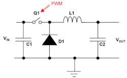
2. The ideal version of the non-synchronous buck SMPS shows the basic components that allow voltage output to be consistently lower than the input voltage.
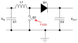
A non-synchronous buck SMPS steps down an input voltage to a lower output voltage level. In its most basic form, the non-synchronous buck SMPS has an input switch, inductor, diode, and capacitor (Fig. 2).
By definition, the non-synchronous buck switcher output voltage (VOUT) is less than the input voltage (VIN) (Equation 1). The establishment of the output voltage is a by-product of the Q1 duty cycle and the inductor (L1) / capacitor (C2) storage capability (Equation 2).
VOUT < VIN (1)
IL-AVE = IOUT (2)
D = VOUT/VIN = t1/(t1 + t2) (3)
where D is the pulse-width modulator’s (PWM) duty cycle applied to the switch.
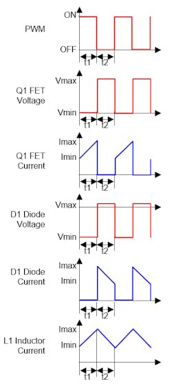
In the non-synchronous buck SMPS circuit, the driving frequency force comes from the PWM signal. The signal’s duty cycle (D) is the percentage of the ratio of t1 to t1 + t2 where the inverse of the sum of these times is equal to the PWM frequency (Fig. 3).
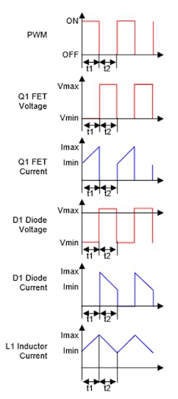
3. Non-synchronous buck timing.
The FET switch (Q1) inversely reflects the transitions of the PWM signal with the PWM off à Q1 closed. At the same time, the diode (D1) is reverse-biased with no current conduction.
The closure of Q1 conducts current to L1 and charges C1 to generate a voltage.
During the PWM t2 time, the FET (Q1) switch opens. At the same time, D1 is forward-biased and pulls current from the inductor to ground. This in turn reduces the C1 voltage.
From this algorithm, you can see that there will be a voltage ripple at the output of the non-synchronous buck SMPS. You can reduce this ripple by increasing the output capacitor (C2) value, but there are boundaries to that. It’s important that the power converter remains stable.
As you compare the non-synchronous buck SMPS to the LDO, the non-synchronous buck will have higher efficiency and low thermal dissipation during operation. In addition, the non-synchronous buck can handle large output currents, especially when the FET switch is on the printed circuit board (PCB). As disadvantages, the non-synchronous buck SMPS is more complicated and will have a high part count. Furthermore, the output voltage switching noise and existing ripple can cause errors in the downstream circuit.
Larger non-synchronous buck SMPS duty cycles produce higher dc output voltages. Looking at Equation 3, the output voltage will always be equal to or lower than the input voltage.
The non-synchronous buck SMPS provides good inductor current filtering because of the inductor-capacitor (LC) arrangement. A continuous switching mode that prevents the inductor current from reaching zero is an ideal condition for the non-synchronous buck SMPS.
Synchronous Buck SMPS
A non-synchronous buck topology is an older design, which is known for its power loss across the diode. This power loss compromises the SMPS’s efficiency.
The synchronous buck SMPS accomplishes an increase in efficiency because the voltage drop across the low-side FET (Q2) can be lower than the voltage-drop across the diode of the non-synchronous buck SMPS. With Q2, the current level through the inductor doesn’t change, a lower voltage drop translates into less power dissipation and higher efficiency (Fig. 4).
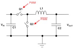
4. The ideal version of the synchronized buck SMPS uses two switches that operate with a PWM non-inverted on Q1 and inverted on Q2 signals.
The synchronized buck SMPS starts with a non-synchronous buck topology. The important distinction is that the second switch (Q2) allows the current to flow in both directions when in the on state.
With the synchronized buck SMPS circuit, the driving frequency force still comes from the PWM signal. The signal’s duty cycle (D) is the percentage of the ratio of t1 to t1 + t2 where the inverse of the sum of these times is equal to the PWM frequency.
The FET switch (Q1) inversely reflects the transitions of the PWM signal with PWM off and Q1 closed. At the same time the diode (Q2) is reverse biased with no current conduction (Fig. 5).
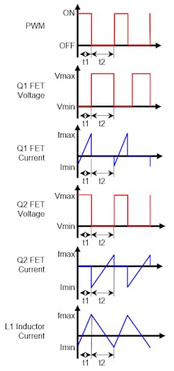
5. Synchronous buck timing.
The closure of Q1 conducts current to L1 and charges the C1 voltage.
During the PWM t2 time, the FET (Q1) switch opens. At the same time, Q2 pulls current from the inductor to ground. This in turn reduces the C1 voltage.
From this algorithm, you can see that a voltage ripple at the output still exists. You can reduce this ripple by increasing the output capacitor (C2) value, but there are boundaries to that as well. It’s important that the power converter remains stable.
As you compare the non-synchronous buck SMPS to the synchronous buck SMPS, the synchronous buck SMPS tends to be smaller and relatively inexpensive. In the synchronous topology, the low resistance (RDS-ON) of Q2 helps reduce losses and optimize overall conversion efficiency. Also, the synchronous buck SMPS circuit is slightly more complicated because of the risk of Q1 and Q2 simultaneously conducting. Timing is everything!
Boost SMPS
The boost SMPS implements a step-up of the input dc voltage; the dc input source can be batteries, dc solar panels, fuel cells, or dc generators. It increases the input voltage to a higher level. A boost or step-up circuit contains the same components as the buck and synchronous buck (Fig. 6).
6. The ideal version of the boost SMPS shows the basic components that allow output voltage to be consistently be higher than the input voltage.
The arrangement of components provides an output voltage that is greater than the input voltage (Equation 4).
VOUT > VIN (4)
IL-AVE = IOUT/(1 – D) (5)
D = (VOUT – VIN)/VOUT (6)
With the boost circuit, the diode (D1) prevents the inductor (L1) current to flow continuously to the output capacitor (C2). With this circuit, the transmission of power to the output is a two-step process. During this two-step process, the inductor serves as a temporary storage element.
The Boost driving frequency force still comes from the Pulse-width-modulator (PWM) signal. The signals duty cycle (D) is the percentage of the ratio of t1 to t1 + t2 where the inverse of the sum of these times is equal to the PWM frequency.
In Figure 7, a closed switch (Q1) causes input current to flow into the inductor with an increase in L1’s magnetic field. During this time the diode (D1) blocks the flow of current to the load. During this time, the output capacitor holds the output voltage steady.
7. Boost timing.
Then, an open switch (Q1) causes the inductor’s magnetic field to fall due to a reverse voltage polarity. This causes current to go to the output and replenish the output capacitance charge and consequently increase the capacitor voltage. This two-step process creates higher peak currents and lower efficiency in higher power applications.
The boost SMPS is a dc-dc converter that steps-up a low dc input voltage to a higher dc output voltage. The boost-converter input device is an inductor, which is an energy storage device. When the switch (Q1) closes, the inductor current flows to ground. When the switch opens, the stored energy continues to generate current, which then flows through the diode to the output capacitor (C1). The inductor current charges the capacitor. One of the by-products of this switching algorithm is an output-voltage ripple.
Characteristics to Consider
There are a few characteristics about these SMPSs to take into account as you move them into your applications. With non-synchronous and synchronous buck converters, the input has a direct connection to a switch (Q1). This causes an interruption to the input current and causes radio-frequency-interference (RFI) noise. As you can see with the capacitor C1 in Figs. 2, 4 and 6, input filtering is in order.
The boost circuit has a rectifier (Q1) blocking the output-capacitor charging current. This causes a much higher ac current in the capacitor, with potential switching noise at the output.
Of all these topologies, the synchronous buck SMPS is the most efficient. This is a nice feature, but be aware—if the step-down ratio is greater than 10:1, the PWM pulses will narrow, causing higher peak currents. The consequence of this is loss that’s proportional to I2.
This is a brief introduction to the more popular SMPS topologies. Please note that these three topologies did not illustrate the functions of the basic controls, such as soft-start, feedback compensation, shutdown, dead-time control, or slope compensation. When selecting your next product, these are issues to consider.
Conclusion
You will find a power-supply conversion in nearly every circuit. This article covers two types of dc voltage conversion: high to low and low to high. When you modify the dc voltage from high to low, you will be using either an LDO or buck converter. The LDO will provide a good linear output at the expense of lower efficiency. You will improve your efficiency with a buck SMPS, but acquire a ripple at the output of the device.
To change a low dc voltage to a higher dc value, the boost topology is appropriate. No linear conversion option is available for this function, but the boost SMPS effectively provides a good solution to this problem.

About the Author
Comment About the Article
To join the conversation, and become an exclusive member of Electronic Design, create an account today!

Leaders relevant to this article: