The Traditional Approach To IC Implementation And Its Problems
Throughout the history of the IC industry, each scaling advance to a new process node has presented a raft of new challenges. In the recent past, relatively straightforward spacing, width, and overlap rules might be tightened up a bit at each node, but in general, these rules did not impact design styles to any large degree. However, at 45 nm and below there are many, many more challenges than we have seen moving from technology node to technology node.
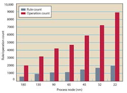
As geometries continued to shrink to well below the lithography exposure wavelength, the interactions between layout features (shapes) became more important and more complicated. This has led to more complex design rules and more complex verification checks to ensure manufacturability. The rule count and average number of verification operations per rule have grown over the most recent technology nodes (Fig. 1).
No longer is it sufficient to observe simple one-dimensional spacing and width rules. Increasingly, systematic manufacturing defects result from the interaction of multiple shapes and their relative position within a context window or area of interdependence. It has become necessary to evaluate complex geometrical functions in multiple dimensions, to identify specific “problem” layout patterns, to measure the effects of chemical mechanical polishing (CMP) on planarity across multiple layers, and to extend checking into the electrical realm, looking at potential electrical interactions in addition to physical ones.
The 45/40-nm node represents a sort of threshold beyond which these emerging design-to-manufacturing interdependencies become critical to achieving optimum functional and parametric yields on a consistent basis across designs. In other words, designers can no longer create layouts using simple rules and hope the process engineers can “fix it on the back end.” The risk of ignoring the full set of complex manufacturing design rules to schedule and yield is too great, and designers are being forced to consider these issues during the design process.
Because of this, the line between design and manufacturing has blurred, and as a result, the line between design completion and manufacturing signoff has become fuzzy as well. This creates a need for a new generation of methods and tools that will help integrate the design and signoff process in a way that ensures manufacturable designs without introducing uncertainty and delays in the development process and without over-burdening the designer.
Impact On Custom And P&R Design Processes
Looking under the covers of traditional design flows reveals where they are breaking down under the increased stress. As an example, both custom and place and route (P&R) IC implementation tools have historically incorporated design rule checkers (DRCs) to ensure the design meets basic rules as the layout is being created. This worked well when the design rules were simple. The designer could expect the layout to mostly meet signoff requirements, except for a few violations that could be fixed by hand using a layout editor or by executing engineering change order (ECO) runs with the P&R tools.
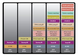
However, with the growing sensitivity of advanced manufacturing processes, designs have to be increasingly constrained with more complex design rules. Some advanced checks are not straightforward layout measurements, but are based on modeling how the manufacturing process will respond to specific combinations of shapes in multiple dimensions and across multiple layers (Fig. 2).
Fig 2. Signoff checks have grown from simple spacing and width measurements to a complex set of models, techniques, and analysis applications
P&R tools by themselves do not perform all the necessary checks to ensure that the design is optimized for manufacturing at advanced nodes. While using simplified design rules for routing worked well at older nodes, at the leading edge they are not good enough and the designer can be left with thousands of violations going into signoff. Even worse, a checker that can’t detect the more subtle violations can’t give the designer any feedback on how to fix the violations.
As a result, designers of advanced ICs and systems-on-a-chip (SoCs) are experiencing an explosion of physical verification (PV) errors that must be fixed before signoff can be completed. This is causing delays in getting designs into manufacturing at the point where schedule pressures are often the most critical.
What Would An Effective Solution Look Like?
What designers need is a design environment that gives them immediate feedback on any violations of the manufacturing rules and requirements and helps them fix problems as the layout is evolving.
One way to do this would be to extend the checkers within the P&R or custom layout tools. However, at advanced nodes this approach is subject to an accuracy gap, i.e., the checking done by the tools does not match the robust verification done at signoff. If the design checking isn’t precisely the same as the signoff checking, the designer still will face a big fixing job late in the development cycle.
The accuracy gap is due to a couple of factors that both contribute to a delay between the establishment of a new design rule by the foundry and its implementation within a custom or P&R design tool. The first factor is the time it takes to implement new design rules in a tool’s technology file or design rule deck once a foundry has determined a need for the rule as it develops its process.
This is a matter of translating the foundry’s design rule manual into the tool’s rule language and then (and this is critical) validating that the rule has been correctly coded and delivers the correct results against the foundry’s regression tests based on test silicon. When there were a few dozen design rules, this delay was minimal and results were easy to test. At today’s advanced nodes, thousands of checks are required, and certifying the results is much more complicated and lengthy.
The second delay factor is the time required to implement new capabilities in the design tool. It is often the case that a new complex rule requires new modeling, measurement, and analysis capabilities in the checker, which takes a significant amount of coding, testing, and validating by the tool vendor. Then customers need to upgrade to the new version of the tool and perform their own certification for their flows.
Beyond matching the foundry design rule manual precisely, the design checking process must also present the same results as the foundry’s reference tool environment. Otherwise, the design might pass all the checks, which theoretically match the foundry’s design rules, but pre-manufacturing acceptance verification at the foundry might reveal discrepancies that result in time-to-volume manufacturing delays.
Basing checking on the same design rule manual does not guarantee accurate results correspondence for many reasons that we will delve into in future editions of this column. It suffices to say that it’s critical that the checker used during design be tested to ensure it delivers the same results as the foundry’s reference verification process.
Because of the inherent accuracy gap, the industry is taking a different approach. Instead of trying to extend the P&R or custom layout tool’s checks, the physical verification and design for manufacturability (DFM) tools themselves are moving into the design environment. This ensures that the advice being given to the layout tool or router will be consistent with the final signoff checking, so a finished design is really finished and signoff (DRC + DFM) clean.
An effective solution must also have good performance and facilities to make it fast and easy to debug both design rule decks and layout violations across all the design teams within a company and across all the suppliers within an IP eco system. It is not realistic to expect overloaded computer-aided design (CAD) and design teams to increase the level of tool support required, nor can they handle a big learning curve, so solutions must also fit the way designers are used to working.
About the Author
Michael White
Michael White is Director of Product Marketing for Mentor Graphics’ Calibre Physical Verification products. Before joining Mentor Graphics, he held various product marketing, strategic marketing and program management roles for Applied Materials, Etec Systems and the Lockheed Skunk Works. Michael received a BS in System Engineering from Harvey Mudd College. He also holds a MBA/BS in engineering management from the University of Southern California.


