Gated Oscillator Starts Without Delay

Download this article in PDF format.
Gated oscillators always present the typical problem of having a delay when a digital input control signal enables its oscillation. This delay happens because the timing capacitor starts discharging from Vdd to start oscillating between two thresholds points known as Vt+, and Vt-. This causes the oscillator to have a time delay before it starts oscillating at its expected base frequency. The delay affects precision in timing measurements.
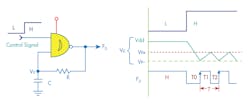
1. This is a classic logic oscillator. The timing diagram is to the right with time periods T0, T1, and T2.
Figure 1 shows a classic gated oscillator with its respective timing diagram. When the control signal goes from low to high logic, capacitor C discharges trough resistor R from Vdd to Vt−, therefore causing a delay called To. In this case, Equation 1 defines the voltage across resistor R during the To interval:
Solving for To, we get:

where Vdd is the NAND’s gate output voltage and VR is the negative threshold voltage Vt− that resistor R will reach. Thus, we get To in Equation 3:

The startup delay To can be eliminated with the solution shown in Figure 2. When the control signal input is low, capacitor C will hold its voltage a few millivolts less than the positive threshold voltage (Vt+) by using a trim pot that will set and hold that voltage. The switching diode D1, will hold the capacitor’s voltage below to Vt+, i.e., < 2.8 V, to avoid triggering the gate. The voltage applied to the capacitor with the trim pot and diode D1 must be less than Vt+ plus Vk, i.e., Vc < (Vt+) + Vk.
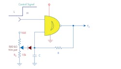
2. This CMOS gated oscillator has no startup delay.
As you can see in Figure 2, when the control signal goes high, the output on NAND gate N1 is low, causing capacitor C to start discharging from Vt+ to Vt−, thanks to the reverse bias in diode D1. The capacitor then will start charging and discharging within Vt+ and Vt− continuously (Fig. 3). When the control signal goes high, the capacitor will go back to its original voltage equal to Vc.
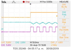
3. The scope image shows the CMOS gated oscillator with no startup delay. The yellow line is the control signal input, the blue line is the capacitor voltage, and the violet line is the NAND gate output.
During the discharging period T2, the switching diode D1 (1N4148 or 1N4150) is reverse-biased and will disconnect the trim pot’s voltage to allow C to discharge up to Vt−. Equations 4 and 5 define the timing periods for charging T1 and discharging T2:


The output frequency Fo is defined by Equation 6:

According to the 74HC132 datasheet, when these NAND gates are biased with Vdd = 5 V, its threshold voltages are Vt− = 1.8 V, and Vt+ = 2.8 V. Substituting these values into Equation 6, we get a constant k in Equation 7:

Notice that the precision of your output frequency depends on the tolerance of the components in the RC network. The resistor tolerance must be 1%. The capacitor tolerance must be 5% or better.
Figure 3 presents the scope image in which you can see how the Capacitor starts discharging from Vt+, (not from Vdd), therefore not causing a delay in the output signal frequency F.
A gated oscillator like this only has a 20-ns delay to start oscillating, defined by the gate propagation delay time Tpd. In this case, we used the Schmitt trigger NAND gate 74HC132. It’s recommended to use the other NAND gates available as buffers to isolate the RC network.
Ricardo Jimenez holds a Master’s in Electronics Engineering, and he is the author of several notebooks on PIC Microcontrollers available at amazon.com.
About the Author
Ricardo Jimenez
Ricardo Jimenez holds a master's degree in electronics from the Instituto Tecnologico de Mexicali.
Comment About the Article
To join the conversation, and become an exclusive member of Electronic Design, create an account today!

Leaders relevant to this article: