Mentorpaper 101907 Image 5eb46d7a07c19

Fusing CMOS IC and MEMS Design for IoT Edge Devices

May 12, 2020
Accommodate single or multiple die techniques for successful IoT edge device design and verification.

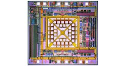
Designers are now creating IoT edge devices that span across analog, digital, RF, and MEMS domains. They are tackling a challenge that once seemed impossible: combining the electronics of the device using the traditional CMOS IC flow with the MEMS sensor on the same silicon die. This paper reveals the secret of how designers accomplish this fusion.

Sponsored

This presentation will provide an overview on proper fan selection, including system profiling, determining a system’s cooling requirements, and an outline of fan types and features...
Discover how 48V systems are being leveraged to reduce overall wiring and accommodate additional power in vehicles.
This video delves into the basics of ultrasonic sensors, including how they work, understanding beam angles, a comparison of strengths and limitations, and more.
How eFuses are helping drive the zone architecture revolution for software-defined vehicles