Header 3 5f317d49a76b3

Application Note: Solving Connection Challenges in On-Wafer Power Semiconductor Device Test

Aug. 10, 2020
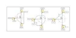
Learn how to minimize connection changes, opportunities for user error, and frustration when performing comprehensive DC I-V and C-V testing of power semiconductor devices.

Measuring DC and capacitance parameters for high power semiconductor devices requires sufficient expertise to optimize the accuracy of various measurements. Even for those with this level of expertise,

managing set-up changes between ON-state, OFF-state and capacitance voltage (C-V) measurements can be time consuming and prone to errors; this is especially true in the on-wafer environment.
Sponsored

Stricter guidelines imposed by version 3 of the IEC standard for harmonic current emissions push designers to embrace power-factor-correction methodologies.
The flyback topology is a versatile, widely used, switched-mode power-supply design with some interesting characteristics that brings performance and BOM advantages to many applications...
Significant complications arise when trying to get your power supply working from a wall outlet.
Login to download this article as a PDF file