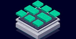
One of the biggest semiconductor engineering challenges is delivering best-in-class devices while dealing with the technology scaling and cost limitations of monolithic IC design processes. To overcome these challenges, more companies are turning to heterogeneous integration and the 3D stacking of ICs and specialized chiplets into 3D ICs. In heterogeneous designs, chips and chiplets are stacked and interconnected with vertical wiring. Designers can also combine them with 3D memory stacks, such as high bandwidth memory, on a silicon interposer within the package of a device.
Learn how to engineer a smarter future faster by downloading this ebook.
This content is sponsored by:

