Knock Out System Noise with Ultra-Low-Noise LDO Regulators
Members can download this article in PDF format.
Low-dropout (LDO) regulators are a simple, inexpensive way to provide a regulated output voltage powered from a higher voltage input. An LDO regulator can regulate the output voltage even when the supply voltage is very close to the output voltage. For instance, it’s able to generate 3.3 V from a 3.6-V Li-on battery. Such regulators are easier to implement than switching converters, and unlike switching regulators, LDOs don’t create high levels of switching noise.
Choosing the right LDO can be critical to maximizing an application’s performance. Low-noise LDOs help ensure a clean dc power supply. It is, as a result, important to both select an LDO with low-noise properties as well as implementing techniques to ensure the cleanest output possible.
Sponsored Resources:
- LDO noise demystified
- How a noise-reduction pin improves system performance
- Clean up your supply rails with the industry's lowest noise LDO
Noise and PSSR
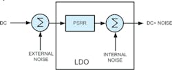
Although an LDO can be simple to implement, its self-generated noise is often confused with its power-supply rejection ratio (PSRR), which measures how much noise from the input couples into the output. Put another way, PSRR is a measure of how well a circuit suppresses extraneous signals (noise and ripple) that appear on the power-supply input to keep them from affecting the circuit output (Fig. 1).
Noise and PSRR are different from each other. Noise is something that may be internal and external to the LDO, whereas PSRR is an internal parameter of the LDO.
PSRR indicates an LDO’s capability to suppress input-voltage ripples. It is expressed as a ratio of output noise to noise at the power supply input, in decibels (dB). Output capacitors and the difference between the input voltage and output voltage are parameters that can affect the PSRR value.
High PSRR over a wide bandwidth enables the LDO to filter switching noise emanating from upstream dc-dc converters. Low-noise (<5 µVRMS) outputs minimize low-frequency noise to maintain the signal integrity of sensitive analog circuitry such as ADCs or DACs, helping generate clean power for precision applications.
A good way to determine PSRR is via the PSRR versus frequency plot that can be found on the datasheet
What Conditions Affect Noise Performance?
Let’s start with the output voltage. Total LDO output-voltage noise consists of input noise that’s coupled to the output, as well as intrinsic noise generated by the LDO.
Because LDOs are electronic devices, they generate a certain amount of noise on their own. Major sources of noise in LDOs are the internal reference voltage and the error amplifier. The reference voltage sets the operating point of the error amplifier. The error amplifier adjusts the resistance of the pass element, which is responsible for transferring current from input to load.
The noise that a system will see is a combination of the internally generated noise of the LDO, plus the noise of the LDO’s power supply. Noise is generated by the transistors and resistors in the LDO’s internal circuitry and by external components.
The type of noise may include thermal, flicker, and shot noise. Transistors generate shot noise and flicker noise. Flicker noise is caused by trapped charges at the gate of the MOSFET. The resistive element of MOSFETs also generates thermal noise. Thermal and shot noise are random in nature and flat over frequency. Unlike thermal noise, shot noise depends on the current flowing and has no relationship to the temperature at which the system is operating.
A common way for noise to sneak into your system is through the power supply. This includes both the power supply for the LDO and the power supply for any amplifiers used to gain up the LDO’s output. To measure the noise that a system will see due to its power supply, the LDO should be powered by the circuitry used in the actual application. A TI application note dives into the nuances of power-supply noise, and provides practical tips for understanding the specifications that may show up in LDO datasheets.
Datasheets commonly provide a single, integrated noise value. Integrating over a select frequency range can help mask certain noise properties, so it’s important to examine the noise curves in addition to the integrated value.
Another good strategy is to employ techniques to ensure that your LDO has the lowest noise characteristics.
For example a noise-reduction pin can improve system performance by filtering reference noise and controlling the slew rate. Many low-noise LDOs in the TI portfolio have a special pin designated as “NR/SS.” This noise-reduction pin filters the bandgap noise using an external capacitor, referred to as the NR cap.
Adding a capacitor at that pin forms a resistor-capacitor (RC) filter, which helps shunt undesirable noise generated by the voltage reference. The function of this pin is twofold. It’s used to filter noise emanating from the internal voltage reference and slow the slew rate during startup.
The most dominant source of noise in an LDO is the internal bandgap. A low-pass filter (LPF) can be inserted between the bandgap output and the input of the error amplifier. This reduces the bandgap noise before it’s gained up by the error amplifier.
Typically, this LPF is formed with an internal resistor and an external capacitor. The cutoff frequency of this filter is set as low in frequency as possible to filter out nearly all of the noise coming from the bandgap.
Clean Up Your Supply Rails with Low-Noise LDOs
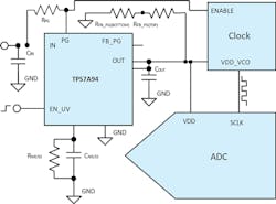
Designers of ultra-sensitive applications such as medical, test and measurement, or telecommunications can leverage an ultra-low-noise (0.46 μVRMS), high-PSRR LDO voltage regulator capable of sourcing 1 A with only 150 mV of dropout. The TPS7A94 (Fig. 2) plus a wide-bandwidth error amplifier allows for very high PSRR (110 dB at 1 kHz and 50 dB at 1 MHz) under low operating headroom (500 mV) and high output current (750 mA).
The device output is adjustable from 0 to 5.5 V with an external resistor. Thanks to its wide input-voltage range, the device supports operation as low as 1.7 V and up to 5.7 V. It can be easily paralleled to achieve lower noise and higher current. Overall, it’s well-suited for powering sensitive analog low-voltage devices.
As we’ve seen, selecting a low-noise LDO and taking steps to reduce internal noise are key to generating clean supply rails. Engineers can find the industry's lowest-noise LDOs in the TI portfolio, including parts whose integrated noise values measure as low as 0.47 μVRMS.
Sponsored Resources:


