The semiconductor singularity: Accelerating IC innovation with AI
Key Highlights
- Read how the hardware-AI feedback loop is driving an exponential leap beyond Moore’s Law.
- Learn why autonomous agents are the key to navigating advanced-node design complexity.
- Learn how to ensure AI-driven workflows remain secure, traceable, and transparent.


The concept of the "singularity" – a point where technological growth becomes uncontrollable and irreversible, resulting in unfathomable changes to human civilization – has long been a staple of science fiction. However, in the semiconductor industry, the idea is rooted in a very real and measurable phenomenon: the recursive feedback loop between hardware and software.
As Ray Kurzweil famously quantified in his "Law of Accelerating Returns," each generation of technology provides the tools to build the next, more powerful generation. In the world of integrated circuits (ICs), this means that more powerful chips enable the development of more sophisticated AI models, which in turn are used to design even more advanced chips. We are not just following a linear path of progress; we are caught in an accelerating spiral that is pushing the industry toward what can be described as the semiconductor singularity.
A century-long feedback loop
Moore’s Law is often credited for the exponential curve in semiconductor capability, but as Kurzweil noted more than twenty years ago, this is just the latest chapter in a story stretching back over a century. From mechanical calculators to relays, vacuum tubes, transistors and finally integrated circuits, each paradigm shift has accelerated the feedback loop. Figure 1 shows a graph created by Ray Kurzweil plotting the exponential increase in computing power over the past 120 years.

Kurzweil’s “120 Years of Moore’s Law,” tracing exponential increases in computing power across successive technology paradigms.
This exponential growth is not limited to a single technology; it emerges from a recursive process where each leap forward is both technical and social. However, as we approach the physical limits of traditional scaling, the industry is facing a new set of challenges. The speed of progress is no longer just about how many transistors we can fit on a die, but how quickly we can navigate the bottlenecks in process integration, IC verification and organizational trust.
Reality check: Bottlenecks in the "inner loop"
Despite the exponential trends in raw compute power, the practical reality of semiconductor design and manufacturing is shaped by significant friction. Moving a design from a software prototype to high-volume production still takes years. Tuning tools for new process nodes, negotiating data access and scaling physical manufacturing all have long, trust-laden lead times.
In the critical domain of IC verification, these bottlenecks are particularly acute. Verification is both the enabler and the gatekeeper of innovation; even the most sophisticated designs stall unless they can be verified quickly, accurately and in a way that builds confidence across organizations. We often feel like we are running fast, but the complexity of modern designs means we are running in molasses. To break through, we need more than just faster algorithms – we need a new form of agency.
The leap: From language models to agentic AI
The latest wave of AI has delivered more than just smarter algorithms; it has brought new forms of agency. While large language models (LLMs) have gained mainstream attention for their ability to answer questions and generate text, the real breakthrough for the semiconductor industry lies in agentic AI.
Agentic AI systems combine LLMs with planning, tool invocation, retrieval, coordination and collaboration. These systems operate across multi-turn objectives, collaborating with both human engineers and other AI agents to solve complex problems. In the realm of IC verification, agentic AI unlocks new levels of productivity by autonomously configuring verification flows, connecting tools across the flow, monitoring power and runtime and flagging exceptions in real time. Figure 2 shows how rapidly AI models like LLMs are closing the gap, moving from simple to complex software tasks in hours instead of days, dramatically easing the developer bottleneck and accelerating the feedback loop.
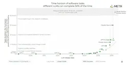
| Jim Shiely | The time horizon of software tasks, showing how LLMs are closing the gap and moving from simple to complex software tasks in hours instead of days.
Imagine a scenario where a designer can simply ask the system to "re-run all signoff checks with yesterday’s updated design data and alert me to any new DRC errors." The agent doesn't just execute the command; it orchestrates the entire workflow end-to-end, implementation to verification. This eases the bottleneck of expert bandwidth, allowing every designer and verification engineer to access scalable expertise without needing to be a tool specialist.
The ultimate bottleneck: Trust and transparency
As we race toward the semiconductor singularity, the integration of AI into the design-to-manufacturing loop brings a critical requirement: these systems must be secure, trustworthy and explainable. Trust remains the ultimate bottleneck in the industry. For AI-driven acceleration to be sustainable, every agent action, every data source used for a rule check and every exception found in signoff must be traceable and auditable.
Teams must have faith not only in the data and methods but also in the transparency and security of their verification flow. This is especially true when sharing critical information with partners and customers. Solutions like Calibre AI by Siemens Digital Industries Software are designed specifically to close this gap, providing a foundation of trust that ensures results are dependable and predictable.
Accelerating the future
The semiconductor singularity is not a distant endpoint but a process we are currently navigating. By removing the barriers of process integration and verification through agentic AI and by embedding trust into every feedback loop, the industry can continue its exponential trajectory.
The goal is to make fast, trustworthy IC signoff and manufacturing a reality, ensuring that as semiconductor technology races forward, we are not just moving faster, but moving with the confidence and transparency required to sustain innovation for the next century.
For more information, please download the white paper “The semiconductor singularity: Accelerating IC innovation with AI”.

Dr. Jim Shiely
Technical and strategic advisor, Siemens EDA
Dr. James P. Shiely serves as a technical and strategic advisor to OPC R&D at Siemens EDA’s Calibre Mask Synthesis group. He holds a Ph.D. in Electrical Engineering with a dissertation in device physics simulation and patents in microlithography simulation and hotspot prediction. He has taught the SPIE course SC1264 “Machine Learning for Lithography” since 2019 and delivered the keynote “Patterning the Singularity” at the 2026 SPIE Advanced Lithography conference. His work focuses on physics-informed machine learning for lithography and the safe adoption of AI tools in software development processes.