Aerosol Jet Prints Skin-Friendly “Tattoos” with Active Electronics
A team at the Duke University Pratt School of Engineering has developed and evaluated a “print-in-place” technique for electronics that’s gentle enough to work on delicate surfaces including paper and human skin. Unlike other so-called “printed electronics” that require multiple layers supported by special treatment after each layer is added, this approach is much more direct. The result is suitable for patches and sensors for biomedical applications including patient-specific biosensors.
“Over the years there have been a slew of research papers promising these kinds of ‘fully printed electronics,’ but the reality is that the process actually involves taking the sample out multiple times to bake it, wash it, or spin-coat materials onto it,” said Aaron Franklin, the James L. and Elizabeth M. Vincent Associate Professor of Electrical and Computer Engineering at Duke. “Ours is the first where the reality matches the public perception.”
Along with Benjamin Wiley, professor of chemistry at Duke, and others, they developed a novel ink containing silver nanowires that can be printed onto any substrate at low temperatures with an aerosol printer (Figs. 1 and 2). It yields a thin film that maintains its high conductivity (low ohmic resistance) without any further processing.
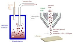
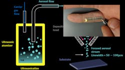
1. The schematic diagram illustrates the working mechanism of an ultrasonic atomizer and aerosol jet printer nozzle. In the ultrasonic atomizer (left), ink is aerosolized via ultrasonication and the ink vial is pressurized by an inert carrier gas flow (N2), which forces the combined aerosolized ink and inert gas flow toward the deposition head. In the deposition head (right), the aerosolized ink flow is focused by an annular inert gas sheath flow (again, N2) and directed toward the substrate. The line printed on the substrate usually has a width between 50 and 100 μm for the inks and nozzle diameters used in this work. Apart from focusing, the sheath flow also avoids the direct contact between the aerosol stream and the inner wall of the nozzle, which reduces the risk of nozzle clogging. (Source: Duke University)
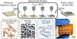
2. Here’s a high-level overview of the process flow and key stages of the “print-in-place” sequence for creating a thin-film transistor (TFT). (Source: Duke University)
After being printed, the ink is dry in less than two minutes and retains this performance even after undergoing a 50% bending strain more than 1,000 times. Check out this quick video of the process and some results:
However, their advance goes beyond the apparently simple but limited function of providing a highly conductive path along the skin surface, as described in the first of two papers, “Silver nanowire inks for direct-write electronic tattoo applications” along with Supplemental Files published in the Royal Society for Chemistry (RCS) journal Nanoscale. A second paper, in the American Chemical Society (ACS) publication Nano, “Flexible, Print-in-place 1D-2D Thin-film Transistors Using Aerosol Jet Printing” and Supporting Information explains how they extended the conductive-ink process to create passive devices such as capacitors (Fig. 3), and even active devices. Combining it with two other printable components led to the creation of functional transistors.
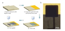
3. The schematic diagram (a) illustrates the fabrication process of a h-BN capacitor: I) masking the Kapton substrate with another piece of Kapton; II) evaporating Au/Cr as the bottom electrode; III) printing the h-BN dielectric layer; and IV) printing the AgNW top electrode. The optical image (b) shows a h-BN capacitor on 127-μm Kapton substrate. (Source: Duke University)
To do so, the printer first puts down a semiconducting strip of carbon nanotubes. Once it dries, and without removing the plastic or paper substrate from the printer, two silver nanowire leads that extend several centimeters from either side are printed. A non-conducting dielectric layer of a two-dimensional material, hexagonal boron nitride (h-BN), is then printed on top of the original semiconductor strip, followed by a final silver nanowire gate electrode.
The result is the creation of 1D-2D thin-film transistors (1D-2D TFTs) in a low-temperature (maximum exposure ≤80°C) full print-in-place process, meaning there’s no need for substrate removal from the printer throughout the entire process. The performance of these devices was evaluated using some of the standard parameters used for FET characterization (Fig. 4). In addition to an ON/OFF current ratio as high as 3.5 × 10⁵, channel mobility up to 10.7 cm2/V-sec, and low gate hysteresis, these 1D-2D TFTs showed extraordinary mechanical stability under bending due to the nanoscale network structure of each layer, with minimal changes in performance after 1,000 bending test cycles at 2.1% strain.
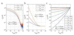
4. Presented in these plots is the electrical performance of an in-place rinsed 1D-2D TFT, including subthreshold (a), transfer (b), and output (c) characteristics. (Source: Duke University)
This work was supported by the Department of Defense Congressionally Directed Medical Research Program (W81XWH-17-2-0045), the National Institutes of Health (1R21HL141028), and the National Science Foundation (ECCS-1542015).
About the Author

Bill Schweber
Contributing Editor
Bill Schweber is an electronics engineer who has written three textbooks on electronic communications systems, as well as hundreds of technical articles, opinion columns, and product features. In past roles, he worked as a technical website manager for multiple topic-specific sites for EE Times, as well as both the Executive Editor and Analog Editor at EDN.
At Analog Devices Inc., Bill was in marketing communications (public relations). As a result, he has been on both sides of the technical PR function, presenting company products, stories, and messages to the media and also as the recipient of these.
Prior to the MarCom role at Analog, Bill was associate editor of their respected technical journal and worked in their product marketing and applications engineering groups. Before those roles, he was at Instron Corp., doing hands-on analog- and power-circuit design and systems integration for materials-testing machine controls.
Bill has an MSEE (Univ. of Mass) and BSEE (Columbia Univ.), is a Registered Professional Engineer, and holds an Advanced Class amateur radio license. He has also planned, written, and presented online courses on a variety of engineering topics, including MOSFET basics, ADC selection, and driving LEDs.
Comment About the Article
To join the conversation, and become an exclusive member of Electronic Design, create an account today!

Leaders relevant to this article: