Heated Microchip Optical Waveguide Enables Tunable Imaging Tomography

The drive to shrink advanced electro-optical medical instrumentation on-chip and in-chip continues along diverse paths. For example, optical coherence tomography (OCT) is a relatively new but now widely used technique to map the back of the eye for disease assessment, such as glaucoma. It’s being extended to other internal-body imaging situations as well.
A brief tutorial: OCT uses time-delay information in the light waves that have been reflected from different depths inside a sample to reconstruct a depth profile of the sample structure. It’s somewhat analogous to ultrasound images. By scanning the light beam laterally across the surface, three-dimensional images can be constructed. With the time-delay information embodied in the light waves reflected from different depths inside a sample, the OCT system can reconstruct a depth profile of the sample structure. It has already become a standard technique for imaging the eye via standard commercial instruments, and there’s active research to apply it to endoscopic imaging of gastrointestinal and cardiovascular systems.
Key to a practical chip-based interferometer-based OCT system is a tunable optical delay line, which is used to determine how the light waves interact. By tuning it to different optical lengths, similar to using different focal lengths in a conventional camera lens, it can collate the interference patterns and thus produce a high-contrast, three-dimensional image.
Now, a team based at Columbia University (with some assistance from Cornell University) has fabricated a coiled and relatively long 0.4-meter delay line of heat-sensitive silicon nitride (Si3N4) into a tiny 8-mm2 area with 720 bends, each with a bending radius of only 80 µm (Fig. 1). Alongside the delay line are integral platinum micro-heaters that effectively tune the optical delay line, thus turning temperature coefficient and associated thermo-optic effect into an advantage. Operating temperature ranged from 0 to 75°C with applied heater power of 0.0 to 0.6 W.
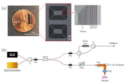
By using the on-board heaters, there are no moving parts and the delay factor is highly stable—a critical factor for achieving image quality. The waveguide is 730 nm deep and 780 nm wide and is designed for single-mode optical performance. Among its impressive optical specifications are near-zero dispersion at 1300 nm along with measured propagation loss of just 0.17 ± 0.01 dB/cm.
Among the problems that had to be overcome were the optical-path losses normally associated with the tight bends of the waveguide, as well as changes in physical size of the bends due to the effect of the heating used for tuning. To overcome this, an optimized fabrication technique was used that one of their members had previously developed, involving tapered regions to precisely “stitch” multiple patterns together.
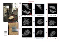
The results of this tunable waveguide approach for OCT included significant improvement in image SNR and contrast (Fig. 2). The on-chip delay line extended the high-SNR imaging depth range by 0.6 mm, increasing the entire imaging range from 2.52 mm to 3.12 mm. While that dimensional change may seem like a trivial amount, it’s a significant difference in this application.
The details of the project are provided in their clearly written paper “On-chip tunable photonic delay line,” published in Applied Physics Letters from American Institute of Physics) along with an Appendix “Device Design and Experimental Methods.”
References
- National Institutes of Health, US Library of Medicine, “Optical Coherence Tomography: An Emerging Technology for Biomedical Imaging and Optical Biopsy”
- The University of Western Australia, “Introduction to OCT”
About the Author

Bill Schweber
Contributing Editor
Bill Schweber is an electronics engineer who has written three textbooks on electronic communications systems, as well as hundreds of technical articles, opinion columns, and product features. In past roles, he worked as a technical website manager for multiple topic-specific sites for EE Times, as well as both the Executive Editor and Analog Editor at EDN.
At Analog Devices Inc., Bill was in marketing communications (public relations). As a result, he has been on both sides of the technical PR function, presenting company products, stories, and messages to the media and also as the recipient of these.
Prior to the MarCom role at Analog, Bill was associate editor of their respected technical journal and worked in their product marketing and applications engineering groups. Before those roles, he was at Instron Corp., doing hands-on analog- and power-circuit design and systems integration for materials-testing machine controls.
Bill has an MSEE (Univ. of Mass) and BSEE (Columbia Univ.), is a Registered Professional Engineer, and holds an Advanced Class amateur radio license. He has also planned, written, and presented online courses on a variety of engineering topics, including MOSFET basics, ADC selection, and driving LEDs.
Comment About the Article
To join the conversation, and become an exclusive member of Electronic Design, create an account today!

Leaders relevant to this article: