Hourglass Fabrication Makes Silicon into More-Responsive Near-IR Photodiode
Silicon-based photodiodes are widely used due to their low cost, low noise, and compatibility with standard IC technologies. However, silicon has a bandgap of 1.12 eV—equivalent to a wavelength of 1,100 nm—making it ineffective for detection of near-infrared (NIR) light (700 to 1,000 nm) as well as short-wavelength infrared (SWIR) light (1,000 to 1,700 nm) because its sensitivity span is narrow and resides only at the edge of the SWIR band.
Now, a team based at Pohang University of Science and Technology (POSTECH) in Korea, working with the NASA Ames Research Center, has developed a new type of silicon photodiode that appears to overcome this constraint. Their silicon photodiodes are based on hourglass-shaped silicon nanowires with so-called “whispering gallery” resonance modes that enhance their near-infrared photoresponse.
"The starting point of this research was to develop a silicon photodetector for power monitoring of laser surgical equipment using a 1,064-nm light source mainly used for ophthalmic applications," noted Professor Chang-Ki Baek, one of the lead researchers.
The initial plan involved adjusting etching gas ratio and time in an attempt to improve absorption at 1,064 nm by changing the diameter and height of the inverted-cone-shaped silicon-nanowire (SiNW) structures they had previously developed. Instead, they found an unexpected appearance in the first hourglass-shaped SiNW array fabricated under certain gas conditions. From previous work, they were aware of two key optical properties of cone-shaped SiNW structures:
- An increase in light absorption in inverted-cone-shaped structures resulting from their resonance.
- A decrease in surface reflectance in regular cone-shaped structures due to their refractive index matching.
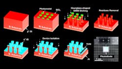
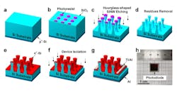
Based on this connection, they predicted that applying an “hourglass-shaped” SiNW array to photodiodes would improve the near-infrared detection. They confirmed this supposition via both simulations and experiments, verifying the improvement of near-infrared detection with their fabricated photodiode. They were able to use standard IC-fabrication techniques for deposition, etching, photolithography, oxidation, and metallization (Fig. 1). The resultant structure is shown in Figure 2.
There were other benefits as well. "In the lower cone-shaped structure, the smaller the diameter, the more similar to the refractive index of air, so the surface reflectance is much lower than that of bulk silicon. Therefore, it can effectively absorb the reflected or transmitted light source from its upper part," said Baek. "As a result, an hourglass-shaped SiNW photodiode can effectively absorb near-infrared, owing to their low surface reflectance and long-effective light absorption length."
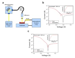
Although many parameters characterize performance and improvement, one important number is the 29% increase in NIR response at 1,000 nm compared to standard silicon photodiodes, reaching a value similar to that of more costly commercial InGaAs photodiodes (Fig. 3). Their device also showed promising performance at 1,400 nm, which is much larger than the bandgap wavelength of silicon.
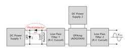
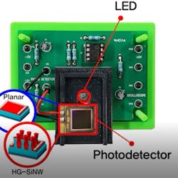
To more dramatically demonstrate the improvement, the team also built a mobile heart-rate measurement system where their enhanced photodiode senses the heart rate and converts it into a voltage (Figs. 4 and 5).
Also, check out this video about the heart-rate measurement system:
In addition to the many medical applications, they foresee applicability to autonomous-vehicle time-of-flight (ToF) LiDAR systems as well as night-vision goggles.
Full details are provided in their paper “Whispering gallery modes enhance the near-infrared photoresponse of hourglass-shaped silicon nanowire photodiodes” published in Nature Electronics, along with additional Supplementary Information. There’s also a crisp, less academic, very readable “Behind the Paper” overview of the team interaction, objectives, path taken, and design rationale in another paper with the same name in Nature Device Materials and Engineering.
About the Author

Bill Schweber
Contributing Editor
Bill Schweber is an electronics engineer who has written three textbooks on electronic communications systems, as well as hundreds of technical articles, opinion columns, and product features. In past roles, he worked as a technical website manager for multiple topic-specific sites for EE Times, as well as both the Executive Editor and Analog Editor at EDN.
At Analog Devices Inc., Bill was in marketing communications (public relations). As a result, he has been on both sides of the technical PR function, presenting company products, stories, and messages to the media and also as the recipient of these.
Prior to the MarCom role at Analog, Bill was associate editor of their respected technical journal and worked in their product marketing and applications engineering groups. Before those roles, he was at Instron Corp., doing hands-on analog- and power-circuit design and systems integration for materials-testing machine controls.
Bill has an MSEE (Univ. of Mass) and BSEE (Columbia Univ.), is a Registered Professional Engineer, and holds an Advanced Class amateur radio license. He has also planned, written, and presented online courses on a variety of engineering topics, including MOSFET basics, ADC selection, and driving LEDs.
