Download this article in PDF format.
Today, links such as PCI Express, HDMI, and USB are ubiquitous. But it wasn’t that way 20 years ago. The last 20 years have seen an explosion in the number of serial-link applications. This article attempts to explain why serial links (and the SERDES that enable them) have become so popular. It will attempt to explain some of the underlying technology that makes serial links ubiquitous, and why that wasn’t the case 20 years go.
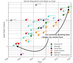
My career began in the late 1990s, just before the serializer/deserializer (SERDES) revolution. In this article, I’ll show examples of some of the SERDES I’ve worked on and use these examples to help explain the progress that the design and technology communities have made in the last two decades (Fig. 1).
Origins and Evolution
SERDES have their background in communication over fiber-optic and coaxial links. The reason for this is quite obvious, of course—sending bytes serially rather than in parallel limits the number of cables! With one or only a few cables, maximizing the throughput over the cable was most important. The SERDES area and power were secondary considerations.
In the mid-1980s, the data rate of serial links was driven in large part by telecom requirements (SONET). During this period, the requirements for OC-1 and OC-3 were modest by today’s standards (51.84 Mb/s, 155.52Mb/s). OC-24 required a line rate above 1 Gb/s (1244.16 Mb/s), which was supported by state-of-the-art circuits around 1990 in bipolar and gallium-arsenide (GaAs) processes.
In the late 1990s, when my career started, it coincided with an important time in the history of SERDES: OC-24 (2488.32 Mb/s) was available and people were planning OC-192 at approximately 10Gb/s. A few years later (early 2000s), 10-Gb Ethernet via a 10-Gb/s line rate became real (as opposed to XAUI, where four channels were used for 10 Gb/s aggregate).
Another important development was beginning—SERDES were being used more and more for chip-to-chip communication on PCBs and backplanes to replace parallel links. This development would turn SERDES from an important long-distance communications circuit into a critical SoC component. Perhaps the most important example of this is PCIe, which was introduced around 2002 at 2.5Gbps and became popular in the mid-2000s.
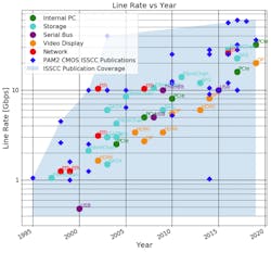
The rollout of various serial data standards and the state of SERDES research is shown in Figure 1. They include:
- Optical transmission: OC-192, OC-768, SONET
- Internal PC: PCIe 1-5
- Storage: Fibre Channel, SATA, SAS
- Serial bus: USB, Thunderbolt
- Video display: DisplayPort, HDMI
- Networking: SGMII, 1-Gb Ethernet, 10-Gb Ethernet, 25/100-Gb Ethernet
As would be expected, line rate has been increasing at an exponential rate. The same effect can be seen across category, with optical transmission leading the other categories. This plot only contains NRZ (PAM2) standards. PAM4 standards are emerging at line rates around 50 Gb/s.
To understand the circuit-level innovations enabling the SERDES evolution, I’ve queried International Solid State Circuits Conference (ISSCC) publications using IEEE’s Xplore Digital Library, generating a list of ISSCC publications covering “Clock and Data Recovery” and “SERDES.” The data set is then broken down by:
- Technology type: CMOS and not CMOS (bipolar, biCMOS, HBT, etc.)
- Geometry: 65 nm, 4 0 nm, 7 nm, etc.
- Signaling: PAM2, PAM4
- Organization publishing: Industrial, academic
Using this data set, the line rate is plotted against the publication year (Fig. 2). It’s estimated that the circuits are designed roughly one year ahead of publication. However, industrial applications following from these publications could trail the publication by several years.
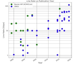
The plot shows that bipolar, biCMOS, and HBT technologies were widely published before 2005, but rarely published following 2005. These pre-2005 publications were describing technologies that drove optical networking applications where line rate was most important, and power/form-factor/integration were secondary considerations.
For SERDES applications with much higher volumes such as PC, storage, video display, and networking, the key isn’t line rate alone. The important factors become cost, power, form factor, and integration with large digital cores.
The plot in Figure 3 is generated by sorting the ISSCC data by academic and industrial publications, and by NRZ/PAM2 vs PAM4 signaling. One thing to note is that the publications above the 28-Gb/s line rate are trending toward PAM4 and that almost no publications below 28 Gb/s are PAM4. This lines up well with the expected future direction of serial data standards.
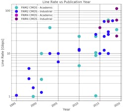
Figure 4 shows the line rate versus the CMOS geometry used. A correlation can be seen between the CMOS geometry and the line rate. For example, below 90 nm, most publications were greater than 10 Gb/s. Also, PAM4 systems weren’t commonly developed or published above 28 nm due to the high level of integration (ADCs, DSPs) needed beyond an NRZ/PAM2 SERDES and the high bandwidth requirements of the CMOS technology.
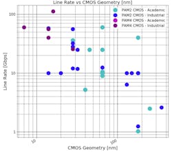
There’s a noticeable lack of PAM4 publications among academic institutions. This is partially due to the search criteria used. There are academic publications related to PAM4 components, but very few full PAM4 transceivers done by academics. One possible explanation for this is the large complexity of a PAM4 system (ADCs, DACs, DSP, PLLs, CDRs, etc.). Another possible explanation is the cost of, and access to, advanced CMOS geometries such as 7 nm and 14/16 nm.
Combining the datasets for serial-link publications and serial-data-rate standards leads to the plot in Figure 5. As can be seen, the advanced CMOS circuit design publications at ISSCC led the way in the high-volume serial data standards from networks to displays by several years. PAM2 CMOS research has made possible PCIe1 through PCIe5 (at 32 Gb/s), 28-Gb/s Ethernet line rates, and more.
Advantages of SERDES
Pin Count and Channel Advantage
The most obvious advantages of SERDES are a reduction in pin count and cable/channel count. For early SERDES, this meant bytes of data could be sent across a coax or a fiber.
For modern SERDES, another advantage is being able to send bytes of data over a pair of differential signal pins rather than 8, 16, 32, or N data pins and a clock pin. This aspect of serialization leads to cost savings due to smaller packages and denser PCBs. The specifics of the advantages depend on die cost, package cost, PCB cost, PCB congestion, and other factors.
Distance Advantage
In the past decade, the ability of SERDES to transmit long distances across PCBs and backplanes has helped them reach many new areas.
From basic microwave design, we know that a transmission line looks like a “lumped element” when the time of flight is less than the rise/fall time. For a parallel interface with GPIOs, the rise/fall times are typically no less than several nanoseconds. This sets the distance that a parallel unterminated interface can operate to about 30 cm on a typical PCB. Terminating a parallel bus would increase the reach; however, it would add a huge amount of power and make the power efficiency drastically worse (Fig. 6).
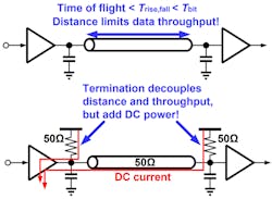
SERDES interfaces are typically transmitting across controlled impedance transmission lines where both ends (TX, RX) are terminated. This allows the bits to be transmitted rapidly without concern for reflections. Of course, to transmit rapidly and serially, a lot of extra complexity is involved—serializers, deserializers, TX PLLs, RX CDRs, feed-forward equalization, receive equalization, etc.
Power Advantage
It’s only recently that SERDES have had a power advantage versus serial data buses. The power consumed by an ideal parallel bus is the power used to charge and discharge the TX and RX capacitances and the trace capacitance. The trace capacitance can be significant on FR4 when distances of 10, 20, or 100 cm are considered.
From first principles, we know that the power for an LVCMOS link is ~C*V^2*f. In the case of data, the frequency is one-half the total bit rate multiplied by the transition density. The total number of transitions and hence power is independent of the number of lanes needed to first order—the more lanes, the fewer transitions per lane. For a 1-Gb/s link, it’s likely that 8-16 lanes would be needed for 10 cm to 1 m. For a 10-Gb/s link, a highly impractical 120 lanes may be needed for 1 m!
Figure 7 shows the power for parallel LVCMOS links of different voltages versus the power consumed by SERDES from the 1990s and today. It can be seen that modern SERDES have a power advantage for longer distances, but the power advantage isn’t clear.
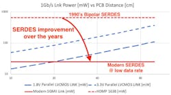
Where SERDES really shine for power is for higher data rates. Figure 8 shows the power for parallel LVCMOS links of different voltages versus the power consumed by various production 28-nm SERDES during the mid to late 2010s. It can be seen that modern SERDES maintain a power advantage for almost all distances. For a power-optimized SERDES, the power advantage is large and clear over all distances.
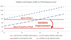
As process technologies advance, the SERDES power advantage continues to grow, of course.
My View of the SERDES Evolution
My career began on the development team of Hewlett-Packard’s discrete SERDES ASICs. The HDMP-1638 was one of the first products I worked on. This ASIC has an “Agilent” label rather than the “HP” label thanks to the Agilent spin-off from HP (Fig. 9).
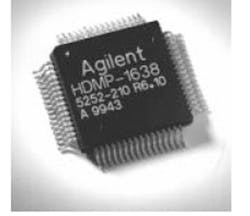
The specifications for this chip were competitive at the time and the sales were good. So I believe this is a reasonable benchmark for an industrial SERDES from 20 to 25 years ago.
This part was designed in a bipolar process. It had a line rate of 1.25Gbps to support Gigabit Ethernet (802.3z), 1000Base-X Gb/s Ethernet over Fiber.
The power dissipation of the HDMP-1638 was about 1 W, which included an external parallel interface—it was a SERDES chip after all! The power dissipation of the chip, excluding the parallel interface, is estimated at 650 mW, or roughly 500 pJ/bit. We’ll come back to the power efficiency (in pJ/bit) later in comparisons with more recent SERDES.
Since 2006, I’ve been at Silicon Creations helping to develop low power SERDES in advanced nodes. In recent years, Silicon Creations has been developing SERDES for up to 32-Gb/s transmission with power efficiency down to 2.5 pJ/bit.
Comparing the speed and power efficiency of these SERDES to the SERDES of 20 years ago:
- Speed is 25X greater
- Power efficiency is 200X better
Again, many factors have contributed to this improvement, including huge advances in technology, voltage scaling, and, of course, good design.
SERDES Challenges
As described in the previous section, SERDES have a compelling advantage for power, pin count, and reach. The disadvantages of SERDES have been the complexity and costs related to SERDES.
Complexity
At a minimum, for low data rates, a good TX PLL, RX CDR, TX driver, and RX front end are needed. Each of these are complex analog subsystems. Designing these blocks and the total SERDES system requires a skilled team of analog/mixed-signal designers to complete. The blocks (along with complex digital control) include:
- A good TX PLL: This block is needed to produce a typically multi-gigahertz clock from a typically 25- to 100-MHz reference clock with very low (~1 ps or better) long-term jitter.
- A good RX CDR: This block is a complex control loop to track the average phase of the incoming data despite any noise, distortion, or crosstalk on the link. This is typically done with either complex phase rotators or a CDR-driven PLL.
- TX line driver: This block translates the serialized data into a typically 50-Ω differential signal, often with precursor and post-cursor emphasis.
- RX equalizer: This block attempts to equalize the high-speed channel effects either with a continuous time equalizer or with a DFE or both. Often an automatic-gain-control (AGC) circuit is needed to facilitate the equalization. The RX equalizer usually includes automatic calibration routines either as state machine logic or as software.
- High-speed serializer and deserializer logic
All of the blocks listed above take considerable design time (up to many person-years) by an experienced design team. As data rates rise (Gb/s) and demands on efficiency grow (pJ/bit), it increases the complexity and cost of the SERDES. As reliability demands increase, a growing number of aging and electromigration simulations must be run and analyzed, further pushing up the cost.
The main focus of this article is on PAM2/NRZ SERDES. PAM4 systems offer alternatives for higher bandwidth per pin, but typically come at the cost of further increases in chip area, power, and complexity over PAM2/NRZ systems.
Fortunately, SERDES have become widely available as IP blocks. Therefore, system companies can license proven designs from leading IP design providers. In this way, the complexity is handled by specialized design teams, and the R&D costs can be shared across multiple chips, projects, and even industries, helping to mitigate costs.
Costs
The major expense of SERDES stems from design (many designers for many total years) and verification, but secondary considerations such as die area and PCB area are important.
SERDES verification at the PMA level is typically handled by the design team, or a subset of the design team. At the system level, verification can be quite complex, especially for standards like PCIe.
For complex serial standards, testbenches (typical in System Verilog) are needed to verify the system from the physical layer (including the PMA and PCS), data-link layer, transaction layer, and device level. Verification covering these levels typically checks protocols, modes, negotiation, error injection and recovery, etc. The verification typically takes many man-months as well, and often involves third-party verification IP (VIP).
On die, a SERDES could potentially be cheaper or more expensive than a parallel interface. Depending on the process node, a SERDES could consume roughly 0.15 to 0.5 mm2 per lane. A parallel interface can be much smaller than this, but would require more I/Os. So, depending on whether the chip is I/O-limited or pin-limited, a SERDES could result in more or less die cost than a parallel interface.
At the package and PCB level, SERDES allow for a reduced pin and trace count. Thus, they should result in smaller and lower-cost packages and PCB designs. However, the design of packages and PCBs using SERDES can be more difficult due to the complexities of high-speed controlled impedance (e.g., 50 Ω) traces and hence more expensive than PCBs using slower parallel interfaces.
Conclusion
The last 20 years have seen SERDES move from an optical and networking circuit to a circuit that’s all around us—from our phones to our laptops and TVs to data centers and more.
PCIe was introduced roughly in 2002 at a 2.5-Gb/s line rate. Since then, design improvements and CMOS process improvements have allowed line rates to improve by ~20X (from ~2.5 Gb/s to ~50 Gb/s) and power efficiency (pJ/bit) to improve by ~200X.
Jeff Galloway is a Co-Founder of Silicon Creations.
About the Author
Jeff Galloway
Co-Founder, Silicon Creations
Jeff is a Co-Founder of Silicon Creations (2006). He has helped start and grow SERDES and PLL product lines along with design centers in Atlanta and Krakow. Before Silicon Creations, he held positions at HP and Agilent Laboratories. His interests include company-wide optimization and IC design. Jeff has 12 U.S. patents. He holds a BSEE from Georgia Tech and an MSEE from Stanford University.
Comment About the Article
To join the conversation, and become an exclusive member of Electronic Design, create an account today!

Leaders relevant to this article: