Across many segments of the market today, interleaving analog-to-digital converters (ADCs) offers several advantages in many applications. In communications infrastructure, there’s a constant push for higher-sample-rate ADCs to allow for multiband, multicarrier radios, in addition to wider bandwidth requirements for linearization techniques like digital predistortion (DPD). In military and aerospace, higher-sample-rate ADCs allow for multipurpose systems that can be used for communications, electronic surveillance, and radar, just to name a few. In industrial instrumentation, the need for higher-sample-rate ADCs continues to increase so that higher-speed signals can be measured more adequately and accurately.
It’s first important to understand exactly what interleaved ADCs are about. To get a better understanding, it’s best to look at what’s actually happening and how it’s being implemented. Then we can explore the benefits of interleaving. Of course, as many know, there’s no such thing as a free lunch, so the challenges of interleaving need to be evaluated and assessed.
About Interleaving
When ADCs are interleaved, two or more ADCs with a defined clocking relationship are used to simultaneously sample an input signal and produce a combined output signal that results in a sampling bandwidth at some multiple of the individual ADCs. Utilizing m number of ADCs allows for the effective sample rate to be increased by a factor of m.
For the sake of simplicity and ease of understanding, we’ll focus on the case of two ADCs. If two ADCs, each having a sample rate of fS, are interleaved, the resultant sample rate is simply 2 × fs. These two ADCs must have a clock-phase relationship for the interleaving to work properly. The clock-phase relationship is governed by Equation 1, where n is the specific ADC and m is the total number of ADCs:
As an example, two ADCs, each with a sample rate of 100 MSPS, are interleaved to achieve a sample rate of 200 MSPS. In this case, Equation 1 can be used to derive the clock-phase relationship of the two ADCs, which is given by Equation 2 and Equation 3:
Now that the clock-phase relationship is known, the construction of samples can be examined. Figure 1 offers a visual representation of the clock-phase relationship and the sample construction of two 100 MSPS interleaved ADCs. Notice the 180° clock-phase relationship and how the samples are interleaved. The input waveform is alternatively sampled by the two ADCs. In this case, the interleaving is implemented by using a 200-MHz clock input that’s divided by a factor of two and the required phases of the clock to each ADC.
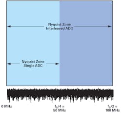
Another representation of this concept is illustrated in Figure 2. By interleaving these two 100-MSPS ADCs, the sample rate is increased to 200 MSPS. This extends each Nyquist zone from 50 MHz to 100 MHz, doubling the available bandwidth in which to operate. The increased operational bandwidth brings many advantages to applications across multiple market segments. Radio systems can increase the number of supported bands, radar systems are able to improve spatial resolution, and measurement equipment can achieve greater analog input bandwidth.
Benefits of Interleaving
The benefits of interleaving span across a range of market segments. The most desired benefit is the increased bandwidth made possible by the wider Nyquist zone of the interleaved ADCs. Once again, using the example of two 100-MSPS ADCs interleaved to create a sample rate of 200 MSPS, Figure 3 gives a representation of the much wider bandwidth allowed by interleaving the two ADCs. This creates advantages for many different applications.
As cellular standards increase channel bandwidth and the number of operating bands, there are greater demands on the available bandwidth in the ADC. In addition, for military applications, the requirements for better spatial recognition, as well as increased channel bandwidths in backend communications, require higher bandwidths from the ADC.
Due to demands for more bandwidth in these areas, accurate measurement of these signals becomes even more crucial. Thus, measurement equipment requires higher bandwidths to properly acquire and measure these higher-bandwidth signals. The system requirements in many designs inherently stay ahead of commercial ADC technology. Interleaving makes it possible to close some of this gap.
The increased sample rate provides more bandwidth for these applications, but also allows for easier frequency planning and reduces the complexity and cost of the antialiasing filter that’s typically used at ADC inputs. With all of these benefits, one has to wonder “What the price do I have to pay?” Though interleaved ADCs offer increased bandwidth and other nice benefits, some challenges also enter the picture in such an implementation.
Challenges with Interleaving
One thing to look out for when interleaving ADCs concerns spurs that appear in the output spectrum, which result from the imperfections associated with interleaving ADCs. These imperfections are basically mismatches between the two ADCs that are being interleaved. Four basic mismatches result in spurs in the output spectrum: offset mismatch, gain mismatch, timing mismatch, and bandwidth mismatch.
Offset Mismatch
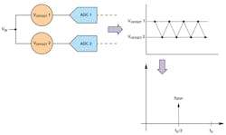
The easiest of these to understand is probably the offset mismatch between the two ADCs. Each ADC will have an associated dc offset value. When the two ADCs are interleaved and samples are acquired alternatively back and forth between the two ADCs, the dc offset of each successive sample changes.
Figure 4 presents an example of how each ADC has its own dc offset and how the interleaved output will effectively switch back and forth between these two dc offset values. The output switches between these offset values at a rate of fs/2, which will result in a spur in the output spectrum located at fS/2. Because the mismatch itself doesn’t have a frequency component and is only at dc, the frequency of the spur that appears in the output spectrum only depends on the sampling frequency and will always appear at a frequency of fs/2.
The magnitude of the spur depends on the magnitude of the offset mismatch between the ADCs. The greater the mismatch, the larger the spur. To minimize the spur caused by the offset mismatch, it’s not necessary to completely null the dc offset in each ADC. Doing this would filter out any dc content in the signal. Furthermore, it wouldn’t work for systems using a zero IF (ZIF) architecture where the signal content is real and complex and includes data at dc.
Instead, a more appropriate technique would be to match the offset of one of the ADCs to the other ADC. The offset of one ADC is chosen as the reference, and the offset of the other ADC is set to match that value as closely as possible. The better matched the offset values, the lower the resulting spur is at fs/2.
Gain Mismatch
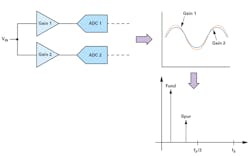
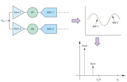
The second mismatch to look at when interleaving is the gain mismatch between the ADCs. Figure 5 represents the gain mismatch between two interleaved converters. In this case, there’s a frequency component to the mismatch. To observe this mismatch, there must be a signal applied to the ADCs.
With an offset mismatch, no signal is necessary to see the inherent dc offset of the two ADCs. With the gain mismatch, there’s no way to see the gain mismatch unless a signal is present and the gain mismatch can be measured. The gain mismatch will result in a spur in the output spectrum that’s related to the input frequency, as well as the sampling rate, and will appear at fs/2 ± fIN.
To minimize the spur caused by the gain mismatch, a strategy similar to that used for the offset mismatch is employed. The gain of one of the ADCs is chosen as the reference, and the gain of the other ADC is set to match that gain value as closely as possible. The better the gain values of each ADC are matched to each other, the less the resulting spur will be in the output spectrum.
Timing Mismatch
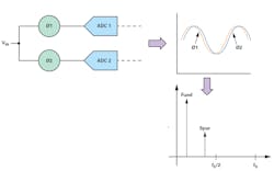
The timing mismatch between the two ADCs has two components: group delay in the analog section of the ADC and clock skew. The analog circuitry within the ADC has an associated group delay, and the value can be different between the two ADCs. In addition, clock skew has an aperture uncertainty component in each of the ADCs as well as a component related to the accuracy of the clock phases that are input to each converter. Figure 6 shows the mechanism and effects of the timing mismatches in the ADCs. Similar to the gain mismatch spur, the timing mismatch spur is also a function of the input frequency and the sample rate and appears at fs/2 ± fIN.
To minimize the resulting spur, the group delay through the analog section of each converter needs to be properly matched with good circuit design techniques. In addition, the clock path designs need to be closely matched to minimize aperture uncertainty differences. Lastly, the clock-phase relationships must be precisely controlled such that the two input clocks are as close to 180° apart as possible. As with the other mismatches, the goal is to attempt to minimize the mechanisms causing the timing mismatch.
Bandwidth Mismatch
The last of these mismatches—the bandwidth mismatch—is probably the most difficult to comprehend and handle. As shown in Figure 7, the bandwidth mismatch has a gain and a phase/frequency component. This makes bandwidth mismatch more difficult because it contains components from two of the other mismatch parameters. In the bandwidth mismatch, however, we see different gain values at different frequencies. In addition, the bandwidth has a timing component that causes signals at different frequencies to have different delays through each converter.
The best way to minimize the bandwidth mismatch is to have very good circuit design and layout practices that work to minimize the bandwidth mismatches between the ADCs. The better each ADC is matched will further diminish the resulting spur. Just as the gain and timing mismatches caused spurs in the output spectrum at fs/2 ± fIN, the bandwidth mismatch also results in a spur at the same frequency.
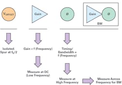
After discussing the four different mismatches that cause issues when interleaving ADCs, a commonality between them emerges. Three of the four mismatches produce a spur in the output spectrum at fs/2 ± fIN. The offset mismatch spur can be easily identified, since it alone resides at fs/2 and can be compensated fairly easily. The gain, timing, and bandwidth mismatches all produce a spur at fs/2 ± fIN in the output spectrum, so the question becomes how to identify the contribution of each. Figure 8 gives a quick visual guide to the process of identifying the sources of the spurs from the different mismatches of interleaved ADCs.
If looking purely at gain mismatch alone, it’s a low-frequency, or dc, type of mismatch. The gain component of the bandwidth mismatch can be separated from the gain mismatch by performing a gain measurement at low frequency near dc and then performing gain measurements at higher frequencies. The gain mismatch isn’t a function of frequency like the gain component of the bandwidth mismatch. A similar approach is used for the timing mismatch. A measurement is performed at low frequency near dc and subsequent measurements are performed at higher frequencies to separate the timing component of bandwidth mismatch from the timing mismatch.
Conclusion
The newest communication system designs, cutting-edge radar technologies, and ultra-high-bandwidth measurement equipment seem to constantly outpace the available ADC technology. Their requirements push both users and manufacturers of ADCs to develop methods to keep pace with these demands. Interleaving ADCs allow for greater bandwidths to be achieved at a faster pace than the traditional path of increasing the conversion rate of a typical ADC. Taking two or more ADCs and interleaving them together increases the available bandwidth, and system design requirements can be met at a faster pace.
Interleaving ADCs does have its challenges, though, and mismatches between the ADCs can’t be ignored. Even though the mismatches do exist, understanding them and how to appropriately deal with them equips designers with the ability to meet the ever-increasing demands of their latest system designs.
Jonathan Harris is a Product Applications Engineer in the high speed converter group at Analog Devices.
Reference
Had, Jim, Mark Looney, and Rob Reeder. “Pushing the State of the Art with Mulitchannel A/D Converters.” Analog Dialogue, Vol. 39, No. 5, May 2005.
About the Author
Jonathan Harris
Applications Engineer, Analog Devices Inc.
Jonathan Harris is a product applications engineer in the High Speed Converter Group at Analog Devices (Greensboro, N.C.). He has over seven years of experience as an applications engineer, supporting products in the RF industry. Jonathan received his MSEE from Auburn University and his BSEE from UNC-Charlotte. In his spare time, he enjoys mobile audio, nitro RC, college football, and spending time with his two children.


