Watch Out, MEMS Switches—Much-Smaller NEMS Relays are Coming After You!
There’s no doubt that devices based on MEMS (microelectromechanical systems) processes and technologies have radically changed the world of sensors and solid-state functions. Since they became commercially viable in the 1980s beginning with analog airbag impact-acceleration sensors—replacing the on/off “ball in tube”—MEMS devices have expanded into sophisticated components ranging from accelerometers and gyroscopes used in drones to RF switches. For example, the ADGM1304 from Analog Devices is a single-pole, four-throw MEMS device with an integrated driver that’s suitable for RF signals from 0 Hz (dc) to 14 GHz.
Among the principles employed by MEMS-based switches (relays) are electrostatic attraction, piezoelectric expansion, and thermal expansion. Despite their fundamental differences, all of these use a flexure structure to provide constraint or restoring force to overcome contact adhesion. However, the required sizing of these flexures prevents MEMS relays from scaling down to dimensions comparable to those of CMOS functions on an IC. Thus, while MEMS switches are much smaller than their discrete mechanical counterparts, they’re still relatively large compared to the size of an IC’s electronic features.
Such a size differential may change, though, thanks to a PhD project at Carnegie Mellon Institute (CMI) that encompassed devising, building, and testing a NEMS switch (the “N” stands for “nano”). It’s based on a different contact principle than MEMS devices—it utilizes a phase-change material (PCM), consequently, it’s dubbed a phase-change NEMS relay (PCNR) device.
“Our goal is to build mechanical switches that are the size of a DNA molecule," said project advisor Professor Gianluca Piazza. "To do so, we are using a solid-state material that, when heated, undergoes a phase transformation and expands by 10%. That is approximately the same volume change that occurs when water freezes. This transformation results in enormous forces and sufficiently large displacements to bridge nanometer-scale gaps and form good electrical contacts as in wall light switches."
For the PCM, the PCNR uses a germanium-tellurium (GeTe) chalcogenide glass (a glass containing one or more chalcogens such as sulfur, selenium, and tellurium, but excluding oxygen). The phase change is induced by an on-chip microheater that melts and quenches the GeTe from the crystalline to amorphous state.
PCNR Construction and Operation
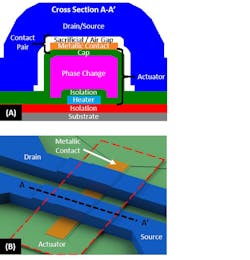
The non-volatile PCNR has two main components: a contact pair and the GeTe phase-change actuator (Fig. 1). The contact pair is created by a metallic contact that’s attached to the top surface of the actuator plus a suspended pair of drain/source contacts. The actuator consists of a resistive heater along with a layer of PCM encapsulated in an insulating cap. The actuator expands and contracts depending on whether the GeTe is in its amorphous (larger) or crystalline (smaller) state, respectively.
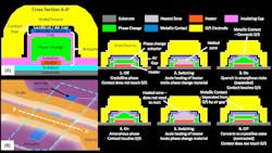
The PCNR operation is a multistep process (Fig. 2). The drain and source electrodes are isolated via an air gap from the metallic contact in its off state and the PCM is in a crystalline state. To flip to the “on” position, the heater melts a portion of the PCM. This heating is then quenched, which converts the PCM to its larger amorphous state. The PCM is liquid for a short period before quenching. (Note that the quench time is important to ensure the PCM remains in the amorphous state; if it cools too slowly, the PCM will crystallize and the relay will not switch to the on state.) The actuator expansion presses the metallic contact into the drain and source and connects them.
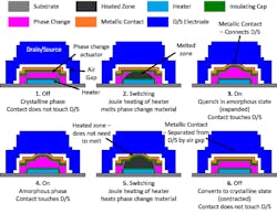
Switching the PCNR to the off state is somewhat more subtle as the PCM isn’t melted. Instead, the heater raises the PCM temperature but without allowing melting to promote rapid crystallization. Thus, the PCM remains solid throughout the process of switching the PCNR to the off state. The crystallization process contracts the actuator, separating the metallic contact from the drain and source, recreating an air gap and thus the off state.
Including heater dimensions, the PCNR is about 1 μm wide by 3 μm long, with an air gap of 20 nm (Fig. 3). Actuator expansion distance is 26 nm, with on/off switching times of 300 ns/600 ns, respectively. There’s still work to be done on basic dc performance, as on-state resistance is 260 Ω and off-state leakage is between 10 and 14 fA.
Further Reading
The details of the project were presented at the 2019 IEEE International Electron Devices Meeting (IEDM) in a paper with the unusually brief title “Phase Change NEMS Relay.” While the paper is behind an IEEE paywall, that’s not a problem in this case as the associated PhD thesis that’s the basis for the conference paper is posted (”Novel Topologies for Highly-Scalable Non-Volatile NEMS Relays” by James T. Best).
At 140 pages, his thesis might seem like too much of a good thing compared to a more-modest conference paper, but there’s no need to worry—it’s very readable, well organized, and explains underlying principles and materials science, COMSOL modeling, fabrication, operation, test arrangements, and more. It also goes beyond details of the PCNR device itself, with plenty of background and even added discussion of other types of MEMS switches in use along with their characteristics and relative attributes.
The PCNR certainly sounds like a perhaps attractive “next-stage” evolution to our widely used MEMS switches. However, anyone who has been involved in new technologies knows that doing something in the lab is very different than having it become a viable, reliable, cost-effective product—just ask any of the engineers who were involved in the early stages of development of MEMS sensors for airbags.
Time and follow-through efforts will tell if NEMS and PCNR succeeds, and whether it will take a few years or decades. Or will it turn out to be another dead-end technology for technical or commercial reasons, despite its apparent cleverness and virtues, similar to all of the “better” battery technologies we see from research labs that just don’t work out in the real world?
About the Author

Bill Schweber
Contributing Editor
Bill Schweber is an electronics engineer who has written three textbooks on electronic communications systems, as well as hundreds of technical articles, opinion columns, and product features. In past roles, he worked as a technical website manager for multiple topic-specific sites for EE Times, as well as both the Executive Editor and Analog Editor at EDN.
At Analog Devices Inc., Bill was in marketing communications (public relations). As a result, he has been on both sides of the technical PR function, presenting company products, stories, and messages to the media and also as the recipient of these.
Prior to the MarCom role at Analog, Bill was associate editor of their respected technical journal and worked in their product marketing and applications engineering groups. Before those roles, he was at Instron Corp., doing hands-on analog- and power-circuit design and systems integration for materials-testing machine controls.
Bill has an MSEE (Univ. of Mass) and BSEE (Columbia Univ.), is a Registered Professional Engineer, and holds an Advanced Class amateur radio license. He has also planned, written, and presented online courses on a variety of engineering topics, including MOSFET basics, ADC selection, and driving LEDs.
Comment About the Article
To join the conversation, and become an exclusive member of Electronic Design, create an account today!

Leaders relevant to this article: