An Intro to JESD204B Subclasses and Deterministic Latency (Part 1)
>> Electronic Design Resources
.. >> Library: Article Series
.. ..>> Series: The JESD204 Story
What you'll learn
- The need for deterministic latency in converter-based applications.
- Three subclasses were introduced in JESD2054B to deal with deterministic latency.
- Implementation methods for subclasses 0, 1, and 2.
Unquestionably, a hallmark of the Information Age is an explosion in the need to collect, process, and distribute larger and larger chunks of data. In communications networks, this means more bandwidth for the infrastructure and the components connecting to it. In the medical industry, this translates into more detailed information from scans, X-rays, and other instruments. Relatedly, testing and analysis of this rapid expansion in bandwidth means the need for higher speed and capacity in electronic test equipment.
This insatiable demand for data is what led JEDEC to introduce the JESD204 standard for a high-speed serial link between data converters and logic devices. The “B” revision of the standard, released in 2011, has pushed the serial-link data rates to 12.5 Gb/s to enable the higher bandwidth requirements of today’s converter-based applications.
In many of those applications, there’s a need for data to traverse through the system with a known and consistent delay from power cycle to power cycle. This concept is referred to as deterministic latency (DL) and provisions for this requirement were introduced in the JESD204B standard as well. Prior to the release of this revision, designers of systems needing deterministic latency used external application-layer circuitry to realize the requirement.
In the JESD204B standard, three subclasses are introduced. Subclass 0 is intended to be backward-compatible with the JESD204A standard and has no provision for implementing deterministic latency. Subclass 1 introduces an external reference signal, called SYSREF, which provides a system-level reference for sample timing. Subclass 2 defines how the SYNC~ signal can be used as the system-level reference for sample timing.
In each case, it’s the sample timing reference that can be used to implement deterministic latency. The intent of this article is to clarify the operational distinctions between the three JESD204B subclasses, as well as provide the reader with a working knowledge on the implementation of their individual deterministic latency functionality.
Designers of systems needing deterministic latency used external application-layer circuitry to implement this requirement prior to the release of this revision.
A Deterministic Latency Overview
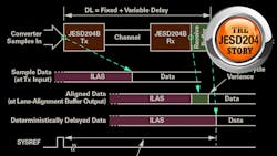
The JESD204B standard defines deterministic latency as the time difference between when frame-based samples arrive at the serial transmitter to when the frame-based samples are output from the serial receiver. Latency is measured in the frame clock domain and must be programmable in increments at least as small as the frame clock period. The latency must be repeatable from power-up cycle to power-up cycle as well as with any resynchronization event. This definition is illustrated in Figure 1.

The deterministic latency in a JESD204 system consists of fixed delays and variable delays. Variable delays are the result of arbitrary phase relationships from power cycle to power cycle between clock domains in the digital processing blocks. In JESD204A and JESD204B subclass 0 systems, the variable delays can’t be accounted for. Therefore, a power-cycle variation exists in the latency across the link.
Subclass 0
Subclass 0 is primarily provided in the JESD204B standard to ensure backward compatibility to JESD204A devices. This could be desirable if system designers have a custom ASIC with a legacy JESD204A interface that they want to connect to a JESD204B converter with updated features.
Requirements from the JESD204B Standard
The JESD204B standard provides requirements and recommendations for operating in subclass 0 mode that may differ from the requirements for the other subclasses. Most notably, the requirements for the SYNC~ signal are unique from subclass 1.
SYNC~ requirements (also applies to subclass 2):
- The SYNC~ output from the JESD204B receiver must be synchronous with the receiver’s frame clock. It’s also required that the transmitter’s frame clock be synchronous to SYNC~; this can be achieved by allowing the SYNC~ input of the transmitter to reset the frame clock counter. The delay from the SYNC~ input to the frame clock boundary must be specified.
- Recommended to use the same logic as for the device clock (LVDS, for example)
- Must not be ac-coupled.
- The device clock to SYNC~ delay (tDS_R) at the receiver device pins must be specified. In a system where the frame clock is faster than the device clock, SYNC~ is launched and captured using the frame clock; regardless, tDS_R is still specified.
- The setup-and-hold times for SYNC~ to the device clock at the transmitter must be specified.
Implications of Subclass 0 Operation
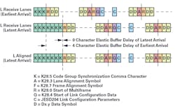
Lane alignment within a single JESD204 link is handled automatically in the JESD204 receiver via an elastic buffer on each JESD204 lane. During the initial lane alignment sequence (ILAS), all lanes are monitored. When the last arriving lane’s start-of-multiframe alignment control character arrives, all buffers are released simultaneously (Fig. 2).
Although it’s recommended that the frame clocks from the receiver and transmitter both be synchronous to the SYNC~ signal (see SYNC~ requirements above), there’s no mechanism to synchronize the local multiframe clocks (LMFCs) across the system. Therefore, link alignment across multiple converter devices isn’t possible using deterministic-latency methods. Conversely, multiple converters within a single device configured as part of a single JESD204B link can be aligned without external circuitry. The LMFC misalignment will contribute up to one LMFC of variable latency to the total latency of the link.
A Subclass 0 Solution for Multichip Synchronization
One advantage of implementing deterministic latency is that it provides a means for multichip synchronization. However, it’s not necessary to implement deterministic latency to achieve multichip synchronization. The JESD204 standard makes provisions for control bits to be added to sample data to convey information about the sample from the transmitter to the receiver.
In ADC applications, it’s possible to use a control bit as a time stamp to flag a sample that occurs coincidently with an external reference. If using a subclass 1 device in subclass 0 operating mode, this can be accomplished using the SYSREF input. It’s also possible to use the SYNC~ signal in multiple-ADC applications connected to a single logic device. The basic requirement for multichip synchronization is to have an external reference for the ADCs and support for control bits in the JESD204 transmitter.
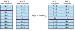
ADI’s AD9625 and AD9680 are devices that support the time-stamp feature for multichip alignment. Figure 3 shows an example of how the SYSREF input can be used to time-stamp the sample that’s coincident with this external reference. As illustrated, when the SYSREF is sampled by the device clock, the designated control bit is set in that sample. This can be done for every device in the JESD204B system.
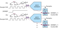
Once the samples from each of the ADC devices are time-stamped, the downstream logic device can align the samples as illustrated in Figure 4.
Subclass 1
Lane alignment within a link and multichip alignment is realizable while operating in subclass 0 mode as previously mentioned. However, many applications depend not only on synchronizing samples from multiple devices, but also require a known, deterministic delay for data traversing between the converter and the logic device.
For example, some ADC applications use a feedback loop to calibrate the front-end analog gain. Oftentimes, this is done using a test input signal into the receiver. The digitized data is then used to determine any adjustments that are needed. It’s critical to know the latency from the analog input to the logic device that’s making the adjustment decision. The arrival time of this data needs to be the same after every power cycle and regardless of synchronization events. In these applications, deterministic latency must be implemented.
In a subclass 0 system, the sample data is released from the JESD204B receiver after the arrival of the latest lane. However, the release time can vary from one power cycle to the next. In a subclass 1 system, a receive buffer is defined and its release time is referenced to the external SYSREF signal. Therefore, it’s not subject to the power-cycle variations that are encountered in the JESD204B system. This concept is illustrated in Figure 5.
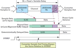
The buffer release time is referenced to the SYSREF signal through its relationship to LMFC. SYSREF is used to phase-align the LMFCs across all of the JESD204B devices in the system. The buffer release time is referenced to this SYSREF-aligned LMFC.
System Requirements and Guidelines for Implementing Subclass 1
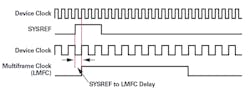
The accuracy and reliability of deterministic latency in the JESD204B system relies on the relationship between the device clock and SYSREF. The device clock is the system reference clock from which the sample clock (typically), JESD204B clock, and serializer clock are derived. It’s used to capture SYSREF and phase-align the leading edge of the frame and multiframe clocks (Fig. 6).
The JESD204B standard provides requirements and recommendations for SYSREF and device clock. The standard also offers guidelines regarding PCB layout and system timing. How these requirements get implemented in a JESD204B system depends on the application’s system-level requirements (deterministic latency uncertainty, or DLU), though.
Other key requirements and suggestions for subclass 1 operation:
- The delay from the leading edge of SYSREF to the frame and multiframe boundary must be specified for all devices in the JESD204B system. In ADI converter products, this is referred to as the SYSREF-to-LMFC delay.
- The receive buffer is used to buffer data and uses the SYSREF-aligned LMFC as a deterministic reference for releasing data. The JESD204B standard defines what’s called the receive buffer delay (RBD). The RBD is what determines the buffer depth and is specified to be between 1 and k frame cycles (TF). The RBD is used to compensate for variable delay in the system. As the number of frames in a multiframe increases, more variable delay can be tolerated. ADI DAC devices support k values of 16 or 32. A setting of 32 is recommended for most applications.
- Since it’s likely that the exact implementation for deterministic latency will vary from one manufacturer to the next, and even different devices from the same manufacturer, it’s important to use the same model of converter when multichip synchronization is required in your system.
- It’s also important that interdevice lane skews be minimized. For ADI DAC applications, the combination of interdevice skew plus the maximum variable delay should be less than the period of the LMFC.
- Device clock and SYSREF should be generated from the same device to ensure the phase alignment of the two signals. The interdevice skew for both the SYSREF and the device clock should also be minimized.
- The concept of SYNC~ combining is presented when discussing subclass 0 operation and multichip synchronization. For a subclass 1 system, this isn’t necessary.
SYSREF and Device Clock
The SYSREF signal can be a single pulse, a periodic square wave, or a gapped periodic square wave. The period of the SYREF must be an integer multiple of the LMFC. ADI devices support all three types of SYSREF signal.
The timing of the SYSREF signal must be accurately controlled with respect to the device clock such that the device clock sampling edge is fixed and known by the user. As already mentioned, the SYSREF signal must be source synchronous with the device clock. Therefore, it’s recommended that SYSREF generation is created by the same device that delivers the device clock throughout the system. The AD9525 is suitable for this task.
The clock-distribution skew and other skew requirements in the JESD204B standard are more like guidelines instead of rules. They were introduced to make a case for the amount of deskew capability to recommend for the deserializer. You can find these described in section 4.12 of the JESD204B standard.
Subclass 2
Rather than utilize an external signal to provide a timing reference, subclass 2 systems use the SYNC~ signal to provide deterministic latency and multichip synchronization. The main advantage to this implementation is that it reduces the pin and net count in the JESD204B system.
Recall that the idea behind SYSREF in subclass 1 is that it’s used to synchronize the internal frame and multiframe clocks across all devices in the system. Since SYNC~ is generated based on the receiver’s LMFC, it carries the LMFC timing information that can be used to achieve the same synchronization between receiver and transmitter as if an external reference were employed. Additional functionality and precision are required for the SYNC~ than that of the subclass 1 SYNC~. These requirements and the system synchronous timing requirements result in lower achievable device clock frequency.
The challenges to meet the timing requirements while using SYNC~ as the timing reference are similar to those when using SYSREF. The system timing accuracy is limited to the distribution skew of the SYNC~ and device clock on the PCB, as well as their propagation delays. The resolution of the accuracy will depend on the device clock period. As with subclass 1, the system DLU requirement will determine the distribution skew limitations.
In a subclass 1 system, the device clock/SYSREF source is the master reference with synchronization requests coming from the logic device. In a subclass 2 system, the logic device is the master timing controller and is responsible for corrections to the LMFC phase on either side of the link. How this is achieved depends on whether the system is a DAC- or ADC-based system.
ADC Subclass 2 Implementation Overview
In a subclass 2 ADC application, the SYNC~ deassertion is captured by the detection clock, which is typically the device clock, and is used to reset the phase of its LMFC. Upon detecting and capturing the SYNC~, besides resetting its local LMFC, the JESD204B transmitter will begin transmitting K28.5 characters and will continue to do so until the system clocks have settled. The ILAS portion of the synchronization process will commence on the LMFC boundary after the clocks have settled.
In an ADC system, the alignment of the ADC’s LMFC isn’t an iterative process and is accomplished with a single SYNC~ assertion (Fig. 7). A periodic SYNC~ can also be used to monitor phase alignment of the transmitter’s LMFC. Refer to section 6.4 of the JESD204B standard for more details.

DAC Subclass 2 Implementation Overview
In subclass 2 operation, the logic device’s LMFC is the master LMFC reference and the converter LMFC must be phase-aligned to it. In a subclass 2 DAC application, the logic device also uses the detection clock (typically, the device clock) to capture the SYNC~ from one or more DAC devices. The logic device will detect the phase difference between its own LMFC and the DAC LMFC and will issue adjustment commands to the DAC during the ILAS portion of synchronization. The ILAS is four multiframes long and the link parameters, including LMFC phase-adjustment information, is transmitted to the receiver during the second LMFC period. The LMFC phase-adjustment commands provided by the logic device to the DAC(s) in the JESD204B system are:
- PHADJ (phase adjust): This command indicates whether a phase adjustment is needed or not.
- ADJCNT (adjustment count): This command indicates the number of adjustment steps that are required.
- ADJDIR (adjustment direction): This command indicates if the LMFC phase should be advanced or delayed.
Depending on the adjustment clock resolution and its relation to the LMFC period, it’s possible that the adjustment of the DAC’s LMFC will take more than one ILAS period. After any phase adjustment is performed on the DAC, it issues an error report by asserting the SYNC~ low. The transmitter on the logic device will use this reassertion to detect the LMFC phase difference again. If no further adjustment is needed, then the PHADJ bit is reset during the ILAS and no error report is issued by the receiver.
At this point, the LMFCs are aligned and user data transmission can commence. If another adjustment is required, the logic device transmitter will initiate another iteration of the process. Refer to section 6.4 of the JESD204B standard for more details.
Once the LMFCs across all of the devices in the JESD204B system are phase-aligned, deterministic latency is achieved through the same methods as subclass 1. That is, the release time of the receive buffer is referenced to the phase-aligned LMFC instead of the nondeterministic arrival time of the last arriving lane data (Fig. 5, again). The only difference is in how LMFC phase alignment is achieved.
System Requirements and Guidelines for Implementing Subclass 2
The accuracy and reliability of deterministic latency in the JESD204B system relies on the relationship between the device clock and each of the SYNC~ signals in the JESD204B system. As with subclass 1, the device clock is the system reference clock from which the sample clock, JESD204B clock, and serializer clock are derived. It’s used to capture SYNC~, which provides information to the logic device regarding the LMFC phase relationships across the system. The JESD204B standard provides requirements and recommendations for subclass 2 operation as summarized below:
For ADCs:
- The ADC must adjust its internal frame clock and LMFC (and possibly sample clock) relative to the detected SYNC~ from the logic device.
- The resolution of the LMFC adjustment should be defined by device manufacture and will limit system synchronization accuracy.
- The SYNC~ detection resolution should be defined by device manufacture and will limit system synchronization accuracy.
- The delay from SYNC~ deassertion to the ADC LMFC boundary as illustrated in Figure 7 must be specified.
For DACs:
- The DAC must be able to adjust its internal frame clock and LMFC as directed by the logic device (as described in the DAC Subclass 2 Implementation Overview section).
- The DAC LMFC adjustment resolution must be specified (in DAC device clock periods).
- The DAC must issue an error report whenever a phase adjustment has been made.
For logic devices in a DAC application:
- They must be able to detect the phase of SYNC relative to its own LMFC in increments of the detection clock (typically the device clock).
- They must be able to calculate ADJCNT based on the DAC adjustment resolution.
- They must be able to send corrective information to the DAC during ILAS.
Final Thoughts
To meet the demands for faster data-processing capability in the applications of today and tomorrow, JESD204B defines the multigigabit interface as a required communications channel between data converters and logic devices. Determining which subclass your application needs is an important step in your system design.
For those systems not requiring deterministic latency, any of the three subclasses will suffice but subclass 0 will be the least problematic to implement. If deterministic latency is a requirement, other system level considerations should be considered for subclass 1 or subclass 2 designs.
Del Jones is an applications engineer for Analog Devices' High Speed Converters Team in Greensboro, N.C.
>> Electronic Design Resources
.. >> Library: Article Series
.. ..>> Series: The JESD204 Story
About the Author
Del Jones
Staff Applications Engineer, Analog Devices
Del Jones is an applications engineer for the High Speed Converters Team in Greensboro, N.C. He has worked for Analog Devices since 2000, supporting ADCs, DACs, and serial interfaces. Prior to ADI, he worked as a board and FPGA design engineer in the telecommunications industry. Del earned his bachelor’s degree in electrical engineering from the University of Texas at Dallas.
Comment About the Article
To join the conversation, and become an exclusive member of Electronic Design, create an account today!

Leaders relevant to this article: