CMOS Plus On-Chip Electro-Optical Interconnect Zooms Past 2 Tb/s
What you’ll learn
- DARPA, Intel, and Ayar Labs collaborate on developing 100-Tb/s-plus in-package silicon photonic interfaces.
- Ayar’s TeraPHY chiplet combines silicon photonics and CMOS in a flip-chip SiP.
- Thermal analysis revealed a method to handle the TeraPHY’s dissipation issue.
There’s a constant reassessment among the three key system blocks—processor, memory, and interconnects (I/O)—which is presently the “choke point” in enhancing overall performance, with each element pushing to get better so as to not encounter undue blame. As processors and memories improve as measured by various metrics, interconnects need to keep up, too, but copper-based links are pushing up against some distinct barriers. Electro-optical interconnects seem like the answer, but getting them to reach their potential as well as work with silicon has been a major challenge.
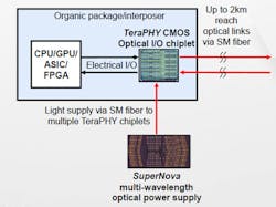
Recently, though, a demonstration showed the dramatic progress made by a collaboration between Intel Corp. and Ayar Labs (Emeryville, Calif.), in a project sponsored by the Defense Advanced Research Projects Agency (DARPA) under its Photonics in the Package for Extreme Scalability (PIPES) program. The goals of this program aren’t modest nor humble, as they look to use advanced in-package silicon photonic interfaces to achieve data rates greater than 100 terabits per second (Tb/s) while requiring energy of less than 1 picojoule (pJ)/bit, as well as be capable of kilometer-scale distances (Fig. 1).

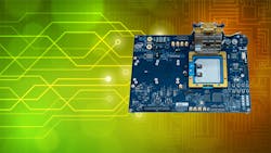
The Intel/Ayar project hasn’t reach those goals, but it did take a significant step toward them. In their virtual demonstration (due to COVID-19) at the Optical Fiber Conference (OFC) 2020, Ayar demonstrated its TeraPHY optical chip technology that was integrated into a modified commercial IC—an Intel Stratix 10 FPGA—that normally uses copper interconnects (Fig. 2).
Developing optical data streams from electronic silicon isn’t a just matter of advanced LEDs, laser diodes, enhanced doping, or unique fabrication structures, albeit all with much-higher performance and twists. Instead, it calls for a new way of thinking, requiring advanced deep electro-optical physics insight involving the relationship among electrons, electric fields, and photons in suitable structures.
Leveraging Silicon Photonics
The basic design is based on using silicon photonics as building blocks including waveguides, directional couplers, and micro-ring resonators. The latter is preferred over the widely used Mach-Zehnder interferometer (MZI) for coupling and energy transfer because it offers approximately 100X smaller footprint, 25-50X higher bandwidth density, and 50X higher energy efficiency. However, it also requires much more complexity in design and precision fabrication.
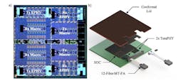
Ayar’s TeraPHY chiplet, which incorporates micron-scale optical waveguides, was fabricated using a 45-nm SOI CMOS fabrication process at GlobalFoundries. The optical waveguides on the TeraPHY chip are etched into the silicon and provide a function that’s the optical analog to copper-based energy and signal paths. Bringing two waveguides in close proximity enables the transfer of photons and thus power from one waveguide to another to create an energy coupler. Within the coupler, a micro-ring resonator with a 10-µm diameter can electrically modulate the phase and control the direction of the light either through or up to the top of the chip, creating I/O drop ports.
The TeraPHY platform consists of monolithically integrated silicon photonics and CMOS (Fig. 3) using a flip-chip system-in-package (SiP) that allows for the combined functionality of an SoC to be split across multiple chiplets in a package. The chiplets are connected together using dense, energy-efficient, and short-reach in-package electrical interconnect.
A key benefit of SiP technology is the ability to enable each chiplet to serve a different specialized function and be fabricated using process technology best suited for accomplishing that function, so long as the chiplet can still conform to standard SiP integration and packaging constraints. This is analogous to using high-density CMOS in a SiP for a processor or FPGA, coupled with a specialty analog processing for precision data acquisition and conditioning.
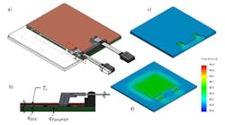
Thermal considerations are as important as electronic and optical ones in a design of this type, despite the 1-pJ/bit objective, as the SoC dissipated 300 W and the TeraPHY dissipated 4.7 W. Analysis showed that a practical solution to the TeraPHY dissipation issue was to separate it into TxRx, electrical I/O, and GPIO regions.
Packaging was also part of the analysis, of course, and the resulting temperature profile illustrates the thermal environment expected in high-performance systems (Fig. 4). While CMOS devices can tolerate these operating temperatures, any co-packaged lasers would have low efficiency and degraded reliability, so the TeraPHY was designed to use an external laser source.
This is only a brief description of what is no doubt a very complicated story. Their three-page OFC paper “TeraPHY: A High-density Electronic-Photonic Chiplet for Optical I/O from a Multi-Chip Module” summarizes the situation. However, its brevity is somewhat frustrating as it can’t delve into context, background, details, or performance. Fortunately, Ayar has also posted a crisp 48-slide PowerPoint presentation, “TeraPHY: A Chiplet Technology for Low-Power, High-Bandwidth In-Package Optical I/O,” which is highly readable and informative about the principles, technology, implementation, and results.
About the Author

Bill Schweber
Contributing Editor
Bill Schweber is an electronics engineer who has written three textbooks on electronic communications systems, as well as hundreds of technical articles, opinion columns, and product features. In past roles, he worked as a technical website manager for multiple topic-specific sites for EE Times, as well as both the Executive Editor and Analog Editor at EDN.
At Analog Devices Inc., Bill was in marketing communications (public relations). As a result, he has been on both sides of the technical PR function, presenting company products, stories, and messages to the media and also as the recipient of these.
Prior to the MarCom role at Analog, Bill was associate editor of their respected technical journal and worked in their product marketing and applications engineering groups. Before those roles, he was at Instron Corp., doing hands-on analog- and power-circuit design and systems integration for materials-testing machine controls.
Bill has an MSEE (Univ. of Mass) and BSEE (Columbia Univ.), is a Registered Professional Engineer, and holds an Advanced Class amateur radio license. He has also planned, written, and presented online courses on a variety of engineering topics, including MOSFET basics, ADC selection, and driving LEDs.
Comment About the Article
To join the conversation, and become an exclusive member of Electronic Design, create an account today!

Leaders relevant to this article: