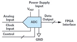
Interfacing FPGAs to an ADC’s Digital Data Output
>> Electronic Design Resources
.. >> Library: Article Series
.. ..>> Series: The JESD204 Story
What you'll learn
- Different types of interface standards used in LVDS.
- Recommendations for interfacing FPGAs to ADCs.
- Methods of troubleshooting when connecting to the AD9268 ADC.
Interfacing FPGAs to ADC digital data outputs is a common engineering challenge. The task is complicated by the fact that ADCs use a variety of digital data styles and standards (Fig. 1). Single-data-rate (SDR) CMOS is very common for lower-speed data interfaces, typically under 200 MHz. In this case, data is transitioned on one edge of the clock by the transmitter and received by the receiver on the other clock edge. This ensures the data has plenty of time to settle before being sampled by the receiver.
In double-data-rate (DDR) CMOS, the transmitter transitions data on every clock edge. This allows for the transfer of twice as much data in the same amount of time as SDR. However, the timing for proper sampling by the receiver is more complicated.
Parallel LVDS is a common standard for high-speed data converters. It uses differential signaling with a P-wire and an N-wire for each bit to achieve speeds up to 1.6 Gb/s with DDR or 800 MHz in the latest FPGAs. Parallel LVDS consumes less power than CMOS, but requires twice the number of wires, which can make routing difficult.
Though not part of the LVDS standard, LVDS is commonly used in data converters with a source-synchronous clocking system. In this setup, a clock that’s in-phase with the data is transmitted alongside the data. The receiver can then use this clock to capture the data easier since it now knows the data transitions.
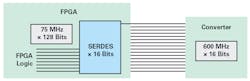
Oftentimes, FPGA logic isn’t fast enough to keep up with the bus speed of high-speed converters, so most FPGAs have serializer/deserializer (SERDES) blocks to convert a fast, narrow serial interface on the converter side to a wide, slow parallel interface on the FPGA side (Fig. 2). For each data bit in the bus, this block outputs 2, 4, or 8 bits, but at one-half, one-quarter, or one-eighth of the clock rate, effectively deserializing the data. The data is processed by wide buses inside the FPGA that run at much slower speeds than the narrow bus going to the converter.
The LVDS signaling standard is also used in serial links, mostly on high-speed ADCs. Serial LVDS is typically used when pin count is more important than interface speed. Two clocks—the data rate clock and the frame clock—are often used. All of the considerations mentioned in the parallel LVDS section also apply to serial LVDS. Parallel LVDS simply consists of multiple serial LVDS lines.
I2C uses two wires: clock and data. It supports a large number of devices on the bus without additional pins. I2C is a relatively slow protocol, operating in the 400-kHz to 1-MHz range. It’s commonly utilized on slow devices where part size is a concern. I2C is also often applied as a control interface or data interface.
SPI uses three or four wires:
- Clock
- Data in and data out (four-wire) or bidirectional data in/data out (three-wire)
- Chip select (one per nonmaster device)
SPI supports as many devices as the number of available chip-select lines. It provides speeds up to about 100 MHz and is commonly used as both a control interface and data interface.
Serial PORT (SPORT), a CMOS-based bidirectional interface, uses one or two data pins per direction. Its adjustable word length provides better efficiency for non-8% resolutions. SPORT offers time-domain multiplexing (TDM) support and is commonly used on audio/media converters and high-channel-count converters. It delivers performance of about 100 MHz per pin. SPORT is supported on Blackfin processors and offers straightforward implementation on FPGAs. SPORT is generally used for data only, although control characters can be inserted.
JESD204 is a JEDEC standard for high-speed serial links between a single host, such as an FPGA or ASIC, and one or more data converters. The latest spec provides up to 3.125 Gb/s per lane or differential pair. Future revisions may specify 6.25 Gb/s and above.
The lanes use 8B/10B encoding, reducing effective bandwidth of the lane to 80% of the theoretical value. The clock is embedded in the data stream, so there are no extra clock signals. Multiple lanes can be bonded together to increase throughput while the data-link-layer protocol ensures data integrity. JESD204 requires significantly more resources in the FPGA/ASIC for data framing than simple LVDS or CMOS. It dramatically reduces wiring requirements at the cost of a more expensive FPGA and more sophisticated PCB routing.
General Recommendations
Some general recommendations are helpful in interfacing between ADCs and FPGAs:
- Use external resistor terminations at the receiver (FPGA or ASIC), rather than the internal FPGA terminations, to avoid reflections due to mismatch that can break the timing budget.
- Don’t use one digitally controlled oscillator (DCO) from one ADC if you’re using multiple ADCs in the system.
- Don’t use a lot of tromboning when laying out digital traces to the receiver to keep all traces equal length.
- Use series terminations on CMOS outputs to slow edge rates down and limit switching noise. Verify that the right data format (twos complement, offset binary) is being used.
With single-ended CMOS digital signals, logic levels move at about 1 V/ns, typical output loading is 10 pF maximum, and typical charging currents are 10 mA/bit. Charging current should be minimized by using the smallest capacitive load possible. This can usually be accomplished by driving only one gate with the shortest trace possible, preferably without any vias. Charging current can also be minimized by using a damping resistor in digital outputs and inputs.
The time constant of the damping resistor and the capacitive load should be approximately 10% of the period of the sample rate. If the clock rate is 100 MHz and the loading is 10 pF, then the time constant should be 10% of 10 ns or 1 ns. In this case, R should be 100 Ω. For optimal signal-to-noise ratio (SNR) performance, a 1.8-V DRVDD is preferred over 3.3-V DRVDD. However, SNR is degraded when driving large capacitive loads. CMOS outputs are usable up to about 200-MHz sampling clocks. If driving two output loads or trace length is longer than one or two inches, a buffer is recommended.
ADC digital outputs should be treated with care because transient currents can increase the noise and distortion of the ADC by coupling back into the analog input.
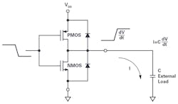
Typical CMOS drivers shown in Figure 3 are capable of generating large transient currents, especially when driving capacitive loads. Particular care must be taken with CMOS data-output ADCs so that these currents are minimized and don’t generate additional noise and distortion in the ADC.
Common Examples
Figure 4 shows the case of a 16-bit parallel CMOS output ADC. With a 10-pF load on each output, simulating one gate load plus PCB parasitics, each driver generates a charging current of 10 mA when driving a 10-pF load.
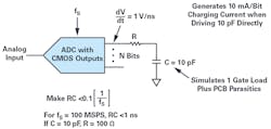
The total transient current for the 16-bit ADC can therefore be as high as 16 × 10 mA = 160 mA. These transient currents can be suppressed by adding a small resistor, R, in series with each data output. The value of the resistor should be chosen so that the RC time constant is less than 10% of the total sampling period.
For fS = 100 Msamples/s, RC should be less than 1 ns. With C = 10 pF, an R of about 100 Ω is optimum. Choosing larger values of R can degrade output data settling time and interfere with proper data capture. Capacitive loading on CMOS ADC outputs should be limited to a single gate load, usually an external data capture register. Under no circumstances should the data output be connected directly to a noisy data bus. An intermediate buffer register must be used to minimize direct loading of the ADC outputs.
Figure 5 shows a standard LVDS driver in CMOS. The nominal current is 3.5 mA and the common-mode voltage is 1.2 V. The swing on each input at the receiver is therefore 350 mV p-p when driving a 100-Ω differential termination resistor. This corresponds to a differential swing of 700 mV p-p. These figures are derived from the LVDS specification.

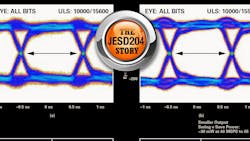
There are two LVDS standards: one is defined by ANSI and the other by IEEE. While the two standards are similar and generally compatible with each other, they’re not identical. Figure 6 compares an eye diagram and a jitter histogram for each of the two standards. The IEEE standard LVDS has a reduced swing of 200 mV p-p as compared to the ANSI standard of 320 mV p-p. This helps to save power on the digital outputs. For this reason, use the IEEE standard if it will accommodate the application and connections that need to be made to the receiver.
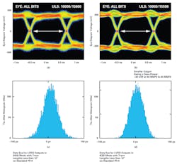
Figure 7 compares the ANSI and IEEE LVDS standards with long trace lengths above 12 inches or 30 cm. Both graphs are driven at the ANSI version standard. In the graph on the right, the output current is doubled. Doubling the output current cleans up the eye and improves the jitter histogram.

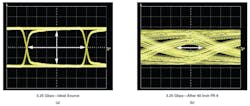
Note the effects of a long trace on FR4 material in Figure 8. The left plot shows an ideal eye diagram, right at the transmitter. At the receiver, 40 inches away, the eye has almost closed and the receiver has difficulty recovering the data.
Troubleshooting Tips
In Figure 9, a VisualAnalog digital display of the data bits shows that bit 14 never toggles. This could indicate an issue with the part, the PCB, or the receiver, or that the unsigned data simply isn’t large enough to toggle the most significant bit.
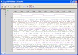
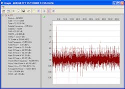
Figure 10 shows a frequency-domain view of the previous digital data, where bit 14 isn’t toggling. The plot reveals that the bit is significant and there’s an error somewhere in the system.

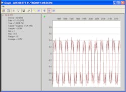
Figure 11 is a time-domain plot of the same data. Instead of a smooth sine wave, the data is offset and has significant peaks at points throughout the waveform.
In Figure 12, instead of missing a bit, two bits are shorted together so that the receiver always sees the same data on the two pins.
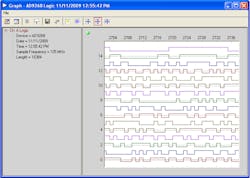
Figure 13 shows a frequency-domain view of the same case where two bits are shorted together. While the fundamental tone is clearly present, the noise floor is significantly worse than it should be. The degree to which the floor is distorted depends on which bits are shorted.
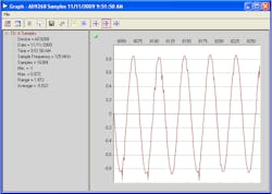
In the time-domain view shown in Figure 14, the issue is less obvious. Although some smoothness is lost in the peaks and valleys of the wave, this is also common when the sample rate is close to the waveform’s frequency.
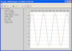
Figure 15 shows a converter with invalid timing, in this case caused by setup/hold problems. Unlike the previous errors, which generally showed themselves during each cycle of the data, timing errors are usually less consistent. Less severe timing errors may be intermittent. These plots illustrate the time domain and frequency domain of a data capture that’s not meeting timing requirements. Notice that the errors in the time domain aren’t consistent between cycles. Also, note the elevated noise floor in the FFT/frequency domain. This usually indicates a missing bit, which can be caused by incorrect time alignment.
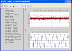
Figure 16 is a closer view of the time-domain timing error illustrated in Figure 15. Again, note that the errors aren’t consistent from cycle to cycle, but that certain errors do repeat. An example is the negative spike on the valley of several cycles in this plot.
Conclusion
This article discussed the standard interfaces—SPI, I2C, SPORT, LVDS, and JESD204A—used to connect an FPGA to an ADC. Interfacing FPGAs to ADCs will continue to be a common challenge as the data rate further increases. JESD204B supports 12.5 Gb/s, and JESD204C moves to 32 Gb/s. Careful design will be required to achieve those high data rates.
>> Electronic Design Resources
.. >> Library: Article Series
.. ..>> Series: The JESD204 Story
About the Author
The Applications Engineering Group
Analog Devices
Comment About the Article
To join the conversation, and become an exclusive member of Electronic Design, create an account today!

Leaders relevant to this article: