Standing on the Shoulders of Mixed-Signal Giants
Editor's Opinionated Note: Yes, the following blog is mostly history, and not technology, but you should probably still pay attention, and tip your hat to these silicon pioneers. The work they did nearly four decades ago is part of the foundation we continue to build the future on.
Can you think back to when wearable devices, such as fitness trackers and Bluetooth headsets, were expensive, bulky, and could only run a few hours on their batteries? Or a time when cell phones were as compact as a size-12 loafer, ate batteries like M&Ms, and did little or nothing besides make calls? Those dark days are a couple of decades behind us thanks to the relentless advance of semiconductor technology, set in motion by the likes of Gordon Moore, Jack Kilby, and Barrie Gilbert, back in the late 1950s and early 60s.
But, while Gordon Moore's well-known "law" gets most of the credit for ushering in the era of ubiquitous electronics, this revolution wasn't just about the number of transistors that can be crammed onto a chip. It also required the development of technologies that allow us to build chips where digital and analog devices peacefully cohabitate on the same device.
Without this second, less well-known evolutionary step, our industry would have never been able to achieve the levels of integration, power consumption, and cost required to make many of the products we take for granted (or make our living designing) possible.
The Groundbreaking BCD Process
Several companies were hard at work developing mixed-signal process technologies back in the early 80s, but the Institute for Electrical and Electronics Engineering (IEEE) recognized STMicroelectronics as the leader in the race when they honored the company with the IEEE Milestone Award for its Bipolar-CMOS-DMOS (BCD) process technology. BCD made it possible to fabricate high-precision bipolar analog transistors, high-performance CMOS digital switching transistors, and high-power DMOS transistors on a single chip.
During the live/virtual ceremony, several of the people who played key roles in the development of the BCD process presented recollections of their work, which began at ST's Italian research centers, located in Agrate and Castelletto. Among the nine scientists, engineers, and project managers who spoke during the live video event were Bruno Murari, the R&D technology director, Paola Galbati, a device process development engineer, and Domenico Rossi, a designer in the special project team.[
The team began by explaining that their research was driven by the recognition that future generations of electronic products would require devices which could deliver electric power in the range of hundreds of watts under the control of digital logic. They also were well-aware these devices would need to be able scale along the seemingly inevitable Moore curve. Furthermore, the devices produced using the new process would have to support precise analog functions and minimize power consumption to eliminate heatsinks.
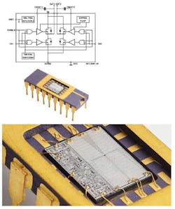
The first commercial BCD device, the L6202 full-bridge motor driver, operated at 60 V, delivering 1.5 A, switching power at 300 kHz and meeting all of its design goals. The new reliable process technology enabled chip designers to flexibly combine power, analog, and digital signal processing on a single die.
While unimpressive by today's standards, it was, as our current president might say, “a big freaking deal.” It not only demonstrated the feasibility of the process, but that the mixed-function chip offered improved power consumption, reduced electromagnetic interference (EMI), a smaller footprint, and lower solution costs.
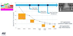
The rest, as they say, is history, as BCD process technology and similar processes developed by other chipmakers have evolved with smaller geometries, innovative transistor structures, and innovative co-packaging techniques. Together, they've helped create the ICs that enabled the advances we've seen in applications such as automotive subsystems, smartphones, home appliances, audio amplifiers, hard disks, power supplies, printers, pico-projectors, lighting, medical equipment, motors, modems, displays, and more.
There's more to the saga, but that's probably about all the history you can afford to indulge in before you get back to your other work. So, I'll close by offering my deep gratitude to all the people honored at the ceremony. In no particular order, please give a virtual round of applause to Bruno Muari, Aldo Romano, Paola Galbati, Claudio Contiero, Claudio Danzi, Domenico Rossi, Gulio Ricotti, Giuseppe Croce, Orio Bellezza, and the hundreds of other engineers, technicians, and managers that made our future possible.
About the Author
Lee Goldberg
Contributing Editor
Lee Goldberg is a self-identified “Recovering Engineer,” Maker/Hacker, Green-Tech Maven, Aviator, Gadfly, and Geek Dad. He spent the first 18 years of his career helping design microprocessors, embedded systems, renewable energy applications, and the occasional interplanetary spacecraft. After trading his ‘scope and soldering iron for a keyboard and a second career as a tech journalist, he’s spent the next two decades at several print and online engineering publications.
Lee’s current focus is power electronics, especially the technologies involved with energy efficiency, energy management, and renewable energy. This dovetails with his coverage of sustainable technologies and various environmental and social issues within the engineering community that he began in 1996. Lee also covers 3D printers, open-source hardware, and other Maker/Hacker technologies.
Lee holds a BSEE in Electrical Engineering from Thomas Edison College, and participated in a colloquium on technology, society, and the environment at Goddard College’s Institute for Social Ecology. His book, “Green Electronics/Green Bottom Line - A Commonsense Guide To Environmentally Responsible Engineering and Management,” was published by Newnes Press.
Lee, his wife Catherine, and his daughter Anwyn currently reside in the outskirts of Princeton N.J., where they masquerade as a typical suburban family.
Lee also writes the regular PowerBites series.


