Stressed-Out Black Phosphorus Becomes Wavelength-Tunable LED, Photodetector
What you’ll learn:
- What black phosphorus is and how it can be stressed to vary its bandgap potential.
- How this attribute was used to build tunable LED photoemitters and photodetectors.
- How the tunable characteristic was lab tested and used to build a multi-gas detector based on a single tunable LED.
Depending on the project and application specifics, engineers have bipolar feelings about stress, which is a force or pressure applied to a material (not to be confused with strain, the resultant dimensional change in that material). On one side, stress is leveraged for very useful applications such as the piezoelectric effect and associated devices. On the other side, stress causes shifts in component performance, and spurs crack growth, fractures, and complete failure.
Now, a team led by researchers at the University of California-Berkeley have found another way to take advantage of stress—they used it to create highly tunable medium-wave infrared (MWIR) light-emitting diodes (LEDs) and photodetectors (PDs). Unlike many electro-optical devices where the wavelength is fixed by material, mechanical, and thermal factors—which is often a desired attribute—there are also cases where the ability to shift wavelength in a controlled manner is a useful feature.
The researchers used the emerging semiconductor material called black phosphorus (bP) to make the two types of optoelectronic devices. Their approach to using bP allows them to tune the bandgap as desired and re-tune back to its original value or to another value within the range.
The ability to use a broader range of the IR spectrum, and be tunable within one device, could be useful in optical communications, thermal imaging, health monitoring, spectroscopy, chemical sensing, and more. To demonstrate this flexibility, the researchers used one of their new devices to detect multiple gases with a single light source (a different wavelength is needed for each to be optically sensed).
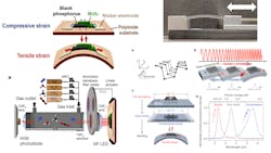
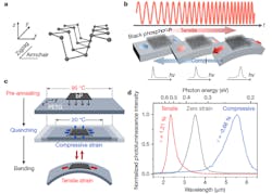
The team used the highly strain-sensitive nature of the bP bandgap, which varies from 0.22 to 0.53 electron volts (eV), to demonstrate continuous and reversible tuning of the operating wavelengths for both LEDs and PDs composed of this material (Fig. 1).
1. Strain-tunable bandgap in black phosphorus: (a) Schematic illustrating the anisotropic crystal structure of bP along the armchair and zigzag directions. (b) Schematic representation of the strain-induced actively tunable bandgap of bP; compressive and tensile strains induce redshift and blueshift of the bP bandgap, respectively. (c) Diagram illustrating the application of strain to bP; compressive strain is applied at 20°C by a thermal expansion mismatch between bP and the substrate, and tensile strain is applied by mechanical bending of the substrate. (d) Normalized photoluminescence spectra of bP under zero strain, compressive strain (ε; 0.66% along the zigzag direction), and tensile strain (ε; 1.21% along the zigzag direction).
What is Black Phosphorus?
Black phosphorus is a two-dimensional material somewhat like graphene. In a process called exfoliation, researchers use Scotch tape (yes, that tape) to lift nanometer-thin layers of the material, which are then transferred to a flexible polymer substrate, in this case polyethylene terephthalate glycol (PETG). (Interestingly, this exfoliation technique is very similar to the one used to create the first monolayers of graphene.)
Due to its puckered lattice structure, bP has unique strain-dependent properties including a bandgap that’s highly sensitive to strain (Fig. 2). Under mechanical strain, bP can be induced to emit or detect infrared (IR) light in a range of wavelengths from 2.3 to 5.5 μm, which spans the very useful short- to mid-wave IR range, and to do so reversibly at room temperature.
2. Strain applied in bP: (a) Photographic image of the two-point bending apparatus used here. An electrical linear actuator that can push/pull one point of the two-point bending apparatus applies a continuous and precise amount of uniaxial tensile strain to bP. (b) Schematic of the two-point bending apparatus. Strain is calculated as ε = t sin θ/a, where ε is the amount of strain; t is the thickness of the substrate; a is the length of the substrate; and θ represents the angle of bending, which is equal to a/(2R) where R is the radius of the curvature. (Note that the circular-arc approximation is not satisfied when θ is large at strains of 20% or more.)
Their paper identifies three accomplishments:
- Development of a continuous and reversible tuning of MWIR electroluminescence using a bP–MoS2 heterostructure on a flexible substrate.
- Extending the detection range of highly responsive bP photodetectors by applying strain.
- Demonstration of actively variable-spectrum optoelectronic devices operating in the infrared regime at room temperature that detect multiple gases (such as CO2, CH4, and H2O) using a single tunable infrared light source.
As noted by team member and postdoctoral fellow Hyungjin Kim, "Because it's mechanically flexible, we can bend it to a desired radius and controllably apply strain to bP." In effect, the bending becomes an effective knob to modulate the bP bandgap. He added that, “In our work, we can actively change the bandgap of the black phosphorous such that a single photodetector or LED can change its operating wavelengths within, roughly, the two- to five-micrometer range,"
Using their techniques, the bandgap shows a modulation rate of 1.70 μm per percent of strain, which they maintain is the highest value reported for direct bandgap semiconductors. This enables a wide modulation of its spectral range without sacrificing performance.
Lab Tests and Field Validation
Assessing the performance of these electro-optical materials is not trivial. Among other factors, they had to separate out the emissions caused by photoluminescence (where a molecule absorbs a photon in the visible region, exciting one of its electrons to a higher electronic excited state, and then radiates a photon as the electron returns to a lower energy state) and electroluminescence (where photons are generated when the excess electron-hole pairs are created by an electric current triggered by an externally applied bias).
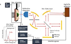
The arrangement for measuring photoluminescence was similar to the one shown in Figure 3 for electroluminescence. The main difference was the use of a laser diode and driver in the photoluminescence test to stimulate the sample under test, in place of the voltage-controlled current source shown for electroluminescence.
3. Setups for measuring electroluminescence: The emission from bP was collected by a reflective objective and sent to the external port of the FT-IR spectrometer, with fmod = 5 kHz, τLock-in = 300 µs, and optical velocity = 0.0633 cm/s.
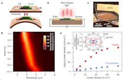
Their paper shows many graphs versus multiple variables, among them Figure 4 for LED performance and Figure 5 for photodetection.
4. Strain-tunable MWIR LEDs based on a bP–MoS2 heterostructure: (a) Schematic showing a strain-tunable bP–MoS2 LED (b) Schematic of the device architecture, showing MWIR electroluminescence under forward bias across the bP–MoS2 heterojunction on a polyimide substrate. (c) Optical micrograph of a representative device. (d) Strain-dependent electroluminescence spectra. (e) Light-current characteristics under 0.20% compressive or 1.06% tensile strain—inset: normalized integrated electroluminescence intensity as a function of emission polarization angle.
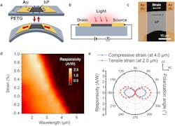
5. Strain-tunable photoconductors based on bP: (a) Schematic of a strain-tunable bP photoconductor. (b) Schematic of the device architecture, showing the generation of a photocurrent at a bias voltage. (c) Optical micrograph of the device: (D is drain, S is source). (d) Strain-dependent spectral photoresponse. (A/W is amps/watt). (e) Polarization-dependent responsivity at 4.0 µm and 2.0 µm for the device under 0.4% compressive strain and 1.0% tensile strain, respectively.
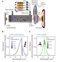
For a real-world “field” test, they used the strain-tunable bandgap of bP to demonstrate an actively variable-spectrum optoelectronic (AVSO) instrument operating in the infrared regime at room temperature (Fig. 6). They maintain that their nondispersive infrared (NDIR) gas-sensing unit, configured as a multiplexed gas-detection system with a single light source. The system is tunable over a broad range to suit various target gases, and has lower operating power, faster modulation, and more rapid stabilization compared to commercial units that need different IR sources to detect different gases (here, H2O, CO2, N2, and CH4).
6. NDIR gas sensing using strain-tunable LEDs: (a) Schematic diagram showing the NDIR gas-sensing system using a strain-tunable bP LED. (MFC = mass flow controller). (b,c) Normalized electroluminescence spectra of a bP LED (0.2%; compressive) in the presence of CO2 gas (b) and a bP LED (0.3%; tensile) in the presence of CH4 gas (c) at different concentrations.
Other coauthors include researchers from the University of Melbourne in Australia. While their paper “Actively variable-spectrum optoelectronics with black phosphorus” published in Nature is behind a paywall, it’s also posted here. There are full details and performance graphs in that primary paper as well as the supplemental material posting which is immediately below that paper.
In addition, a brief video shows dynamic emission spectrum tuning of bP-LED. This work was supported by the U.S. Department of Energy, the Defense Advanced Research Projects Agency, and the Australian Research Council.
About the Author

Bill Schweber
Contributing Editor
Bill Schweber is an electronics engineer who has written three textbooks on electronic communications systems, as well as hundreds of technical articles, opinion columns, and product features. In past roles, he worked as a technical website manager for multiple topic-specific sites for EE Times, as well as both the Executive Editor and Analog Editor at EDN.
At Analog Devices Inc., Bill was in marketing communications (public relations). As a result, he has been on both sides of the technical PR function, presenting company products, stories, and messages to the media and also as the recipient of these.
Prior to the MarCom role at Analog, Bill was associate editor of their respected technical journal and worked in their product marketing and applications engineering groups. Before those roles, he was at Instron Corp., doing hands-on analog- and power-circuit design and systems integration for materials-testing machine controls.
Bill has an MSEE (Univ. of Mass) and BSEE (Columbia Univ.), is a Registered Professional Engineer, and holds an Advanced Class amateur radio license. He has also planned, written, and presented online courses on a variety of engineering topics, including MOSFET basics, ADC selection, and driving LEDs.
Voice Your Opinion!
To join the conversation, and become an exclusive member of Electronic Design, create an account today!

Leaders relevant to this article:
