Pain Points for RF Product Design
What you'll learn:
- Main challenges facing RF designers.
- Design issues regarding PCBs, 5G, and regulations.
- Difficulties in finding RF engineering talent.
Having been involved in developing products in virtually every product category from consumer to medical to commercial to DoD/aerospace, we’ve discovered that in every case requiring wireless technology, one comes across the seemingly black art of RF system design. Such engineering requires a high level of experience to solve tough problems involving strong fundamental expertise in physics.
The problem set in RF design spans the gamut from implementing active wireless communication technologies (transmit and receive) like satellite, cellular, Wi-Fi and Bluetooth, to passive RFID tagging used in applications such as NFC payment systems or tagging of retail items like clothing. RF system design also includes UL- and FCC-related issues, robust circuit design, and good PCB layout to minimize unintentional radiated emissions and low susceptibility to outside interference. Because of the latter, RF system design is a factor in just about anything with a wire attached to run power.
Listed below are five of the unique RF challenges in the development of technology products:
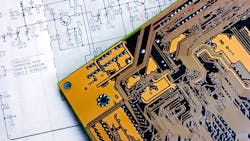
1. Issues related to PCB design
Design of a PCB, especially high-density and mixed-signal boards, presents a big challenge in system design. While physically larger/lower-density boards may be able to leverage off-the-shelf or reference antenna designs, in cases when circuits are compressed, there may not be easy antenna solutions.
Antenna configuration and placement is a major factor in radio performance. In many handheld and mobile products, severe space constraints make it difficult to incorporate efficient antenna operation due to limitations on antenna size. This can drive the need to use small chip antennas, for example. For monopole antennas such as chip antennas and quarter-wave whip antennas, the PCB ground plane is needed to form the counterpoise half. As a result, PCB size constraints can make it challenging to optimize antenna efficiency and communication range.
In a host of products, the current crop of systems-on-a-chip with integrated radios and antennas are ideal solutions. However, these come with their own challenges especially in high density systems. Such modules are not necessarily optimized for size compression. They also present difficulties in PCB layout when using existing reference designs.
2. Multiple radio systems
The more radios in the system, the more antennas and more intricate the antenna design. This presents challenges in board layout that affect performance and crosstalk noise-related issues that are difficult to resolve. With close placement of antennas, interference between cellular and Wi-Fi can be an issue implying the need for careful antenna placement, orientation, and filtering techniques.
3. 5G system design
Everyone is jumping on the 5G bandwagon for many of the right reasons. 5G builds upon the existing technologies and frequency bands of 4G, but also adds a new band of frequencies in the region of 25 to 40 GHz for super high-speed communication applications. However, high-frequency 5G systems present design and application challenges.
Due to the high frequency, performance is impacted by reduced range—high frequencies don’t penetrate the environment as well as lower frequency ranges. It’s a tradeoff between range, bandwidth, and transmission rates when considering 5G implementation. For example, to ensure super-high-speed data rates at these high frequencies, a high base-station density and line-of-sight communications will be more important and will increase infrastructure costs.
4. System design and regulatory issues
The obvious domain for RF designers is in radio integration. However, such engineers also are called upon to debug problems in passing regulatory requirements. Virtually every product with a wire has run into challenges passing the radiated and conducted emissions and susceptibility requirements.
Systems in the corporate lab not impacted by noise get into the agency approval process and find noise problems that can be traced to things as simple as cable layout. RF engineers must assist in design of robust guard-band on emissions and susceptibility to ensure variances in the test setup don’t result in failures. Such failures can be a killer due to additional redesign cost, additional agency lab time, and the delay in time to market.
It’s crucial to engage RF engineers early in the design and product requirements stage to ensure PCB design, layout, and shielding is up to snuff. For example, making sure a design has sufficient capacitance, good power/ground plane layout, and good signal trace routing is necessary to minimize spurious emissions and contamination of the circuits from external noise sources. Oftentimes, cables are a cause of spurious emission failures, too, due to them carrying common-mode currents that need special attention, such as cable placement filtering and shielding techniques.
5. Finding the talent
Good RF engineers must have a strong background in both electrical engineering and physics. Not only is the competition for experienced talent fierce, but there’s a scarcity of RF-focused engineers being turned out of engineering colleges and universities. RF engineering is sometimes viewed as a mysterious skill set somewhere between engineering and science. The pipeline for staff is small and doesn’t appear to be improving any time soon. (By the way, this is good news for those considering an EE career in the domain of RF.)
Almost any company developing electronic systems, whether or not they have wireless communications, needs access to an RF expert either on the team or on standby to call in when needed (and they will be needed). Few, if any products sail through UL and FCC testing unscathed—even those designed with the benefit of a highly skilled and experienced EE or RF designer. In no engineering discipline does this phrase apply better: You have to understand the physics of the problem.
At IPS, we’re fortunate to have a sub-team of highly experienced and technically proficient RF and antenna system designers. They’re worth their weight in gold. Without such talent, one can spend inordinate amounts of time designing and testing to get a high-performing (or even minimally satisfying) result that secures regulatory approval for product sales in a developed country.
About the Author
Mitch Maiman
President and Cofounder, Intelligent Product Solutions
Mitch Maiman is the President and Cofounder of Intelligent Product Solutions (IPS), a leading product design and development firm. He honed his deep knowledge of product design on the strength of a 30-year career with companies that manufacture commercially successful products for the consumer, industrial, and DoD markets. Prior to launching IPS, Mitch was VP of Engineering at Symbol Technologies.
Always espousing a hands-on approach to design, he holds a portfolio of numerous United States and international patents. Mitch holds a Bachelor of Science from Hofstra University, a Master of Science in Mechanical Engineering from Columbia University, and an MBA from Fairleigh Dickinson University.
Comment About the Article
To join the conversation, and become an exclusive member of Electronic Design, create an account today!

Leaders relevant to this article: