How to Shield Your 5G Systems from EMI

This article is part of the TechXchange: Delving into EMI, EMC and Noise
Members can download this article in PDF format.
What you'll learn:
- Open-aperture vulnerabilites in various use cases.
- Methods involved in conformal EMI shielding.
- Results from a study comparing conformal coating and compartment technologies.
5G system hardware designers are challenged to implement better power solutions that help all necessary electronics to fit into form factors close to those of existing 4G base-station enclosures while maintaining a low EMI.
Increased board component density in 5G systems demands space-saving solutions with higher efficiency and lower EMI than traditional discrete dc-dc ICs with external inductor-based solutions. This will challenge designers to create a careful layout of components for filters to minimize radiated and conducted EMI generated via power converter and inductor switching currents.
It’s no secret that dc-dc converters are notorious for conducted EMI coming from magnetic fields emanating from the current loop path. That path is comprised of the output switching node to ground as well as the input capacitor to ground.
Radiated EMI also is generated from the MOSFET switching node to the connection at the inductor. This creates high dV/dT because it’s continuously switching from the high input voltage level to ground as well as from inductor-generated electromagnetic fields.
This system design may lead to multiple, costly EMI lab tests in order to meet the standard. An integrated module may be a better option here.
5G EMI Shielding
5G is an awesome technology. Applications in a 5G system can range from smartphones, healthcare, and vehicle-to-everything (V2X) to smart appliances, public safety, and much more. However, one improper shielding device failure could cause a larger communications snafu that possibly affects a broader system disruption.
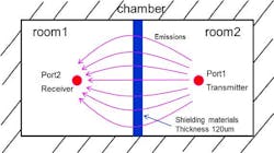
Designers must avoid open apertures as well as non-conductive regions that diminish the overall electronic enclosure. They allow EMI and RFI to exit the design areas to the outside or enter the system design area to possibly cause the system to malfunction or even fail.
One of the main open apertures and non-conductive regions is cable entry, particularly vulnerable near connectors. Power and signal access panels could contribute to EMI problems here. And finally, viewing windows, as well as heating, ventilation, and air conditioning (HVAC) vents, can be access areas that EMI may enter or exit.
Some other potentially vulnerable use cases include:
5G in the military
Military enclosures will need to pass MIL-STD-461, possibly requiring 60-dB, 80-dB, or even higher attenuation levels to achieve compliance. To achieve such levels of electromagnetic shielding attenuation, open apertures and non-conductive areas may not be larger than a few thousandths of an inch.
5G in the medical arena
EMI in some sensitive medical applications could harm a patient or even cause death. Medical facilities must properly shield operating theater equipment, as well as other areas that need protection, such as where imaging devices are in use.
EMI Shielding in Package Module Designs
System-in-package (SiP) module design, and associated assembly technology, plays a key role in IoT, antenna-in-package (AiP), and RF modules. High-speed data transmission and low latency are prime characteristics for 5G RF systems.
Now let’s look at EMI coating and partition technology in SiP modules.
EMI Coating
Conformal EMI shielding can be implemented using a metal frame, sputter coating, or spray coating technology to prevent disturbance in an electronic circuit. Unfortunately, though a basic metal frame shield is good, it doesn’t always provide the best performance.
A SiP with an EMI shielding structure is absolutely the most innovative technology in a 5G RF system. In the mobile computing market, antennas also are integrated in the SiP module to minimize board footprint.
A 3D SiP solution employs a double-side molding technology and AiP architecture. In 5G, AiP technology has been widely applied in many IoT, RF module, and wireless transmission applications.
For 5G millimeter-wave (mmWave) generation, which operates at frequencies higher than 28 GHz, the antenna wavelength is suitable for small package sizes. This small size presents challenges in AiP design, such as EMI shielding technology, partition design, low-loss substrate material selection, and multi-layer substrate antenna design capability. Partition EMI shielding technology is used to isolate different function blocks in the SiP module.
Copper/SUS (“steel use stainless” or stainless steel) sputter coating is a popular coating method used within assembly industries. A 3- to 5-µm thickness coating has ideal shielding performance as well as very good particle adhesion on coating surfaces.
To facilitate a more flexible shielding design between the different function blocks in a SiP, compartment shielding technology is proposed to isolate the signal noise between the digital and RF/analog circuits within the SiP module.
A metal-frame partition design has the advantages of simple assembly, lower cost, and good shielding effectiveness (SE) for the low frequency spectrum. However, the SE may degrade in the mmWave range due to possible jagged solder pad design. As a result, epoxy filling is becoming a more popular shielding design that supports a flexible partition shape and good SE performance in mmWave signals.
Comparing EMI Shielding in Conformal Coating and Compartment Technologies1
EMI shielding technology, in both conformal and compartment methodology, using the simulation model and real device methods, were shown the same trend and result in an experiment. A test vehicle (TV) was designed with an advanced SiP module employing antenna integration and partition EMI shielding technology. The TV of a compartment SiP module, with a 650-mm2 package size and 1.4-mm molding thickness, designed using metal frame and epoxy filling partition technology, is shown in the table.

In this study, the first stage of a 3-µm metal coating conformal shielding technology, in a 10- × 10-mm package size, involved in a single unit and a side-by-side coupling simulation (see figure).
Results demonstrated a marked improvement of SE in the dc to 6-GHz frequency range. Also, the ferrite coating plate was covered on the RF die, and the copper was coated onto the molding compound by sputter technology. The SE improved below the 6-GHz frequency band due to the intrinsic cutoff frequency characteristic of the ferromagnetic material.
Compartment shielding also was demonstrated in this study. The metal frame and conductive epoxy were applied in the simulation model and in the real device. The metal material demonstrated better SE performance in this experiment. According to the SE calculation formula, the SE is proportional to the electric conductivity of the material, which dominated by skin effect. Based on the calculation result, the SE of Cu-Ni is 8.3X better than conductive epoxy, which is compatible to the simulation condition.
Finally, to verify the SE between the materials of metal, epoxy, and SUS + Cu, with and without the hole on the bottom of the shielding wall, the AiP with partition structure was designed and tested. Both the metal frame and SUS + Cu coating solution improved over 35 dB SE between the 25- and 45-GHz frequency bands due to better conductivity properties.
In summary, the package level reliability was tested by the JEDEC standard, which included the MSL 3, TCT1000, u-HAST96, and HTS1000 test conditions.
Conclusion
No one unique shielding solution is perfect for every EMI problem. Architects and designers need flexible material options when EMI plagues challenging designs. Designers need flexibility in their solutions, which can target board- and enclosure-level EMI problems. For very challenging designs, designers may want to combine multiple options to create a custom solution.
References
1. EMI Shielding Technology in 5G RF System in Package Module, 2020 IEEE 70th Electronic Components and Technology Conference (ECTC)
EMI Mitigation at Millimeter Wave, Proceedings of the 1st European Microwave Conference in Central Europe
Innovative EMI Shielding Solutions on Advanced SiP Module for 5G Application, IEEE 2019
About the Author

Steve Taranovich
Freelance Technical Writer, Phoenix Information Communication LLC
Steve is a contributing editor to Electronic Design.
Author of the non-fiction “Guardians of the Right Stuff,” a true story of the Apollo program as told by NASA and Grumman Corp. engineers, an astronaut, and technicians.
Experienced Editor-In-Chief of EETimes/Planet Analog and Senior Technical Editor at EDN running the Analog and Power Management Design Centers from 2012 to 2019.
A demonstrated history in electronic circuit design and applications for 40 years, and nine years of technical writing and editing in industry. Skilled in Analog Electronics, Space-related Electronics, Audio, RF & Communications, Power Management, Electrical Engineering, and Integrated Circuits (IC).
1972 to 1988 worked as a circuit design engineer in audio (8 years) and microwave (8 years). Then was Corporate Account Manager/applications engineer for Burr-Brown from 1988 to 2000 when TI purchased Burr-Brown. Worked for TI from 2000 to 2011.
Strong media and communication professional with a BEEE from NYU Engineering in 1972 and an MSEE from Polytechnic University in 1989. Senior Lifetime member of IEEE. Former IEEE Long Island, NY Director of Educational Activities. Eta Kappa Nu EE honor society member since 1970.
Comment About the Article
To join the conversation, and become an exclusive member of Electronic Design, create an account today!

Leaders relevant to this article: