Increase System Accuracy and Efficiency with Precision Op Amps
Members can download this article in PDF format.
The precision op amp plays a key role in analog and mixed-signal circuits. Applications extend from measuring large currents by amplifying the voltage across a low-side shunt to serving as a transimpedance amplifier (TIA) with a photodiode input. You can speed your way to successful op-amp designs if you understand subtle distinctions in parameters such as slew rate and small-signal rise time, minimize errors related to gain and nonlinearity, and adhere to basic PCB layout guidelines.
Slew Rate vs. Bandwidth
Figure 1 shows a precision OPA391 op amp configured to measure the voltage across a 400-mΩ shunt in response to a 100-A current through it. The op amp, with a 100-kΩ feedback resistor and a 1-kΩ input resistor (for a gain of 101 V/V), amplifies the 40-mV drop across the shunt to produce a 4-V output.
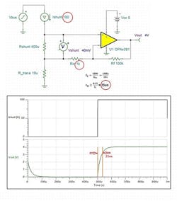
A key question is: How long will it take the op-amp circuit to reach the 4-V level after a 0- to 100-A current step? You might consult the OPA391’s datasheet and, based on the specified 1-V/µs typical slew rate, predict that it would take about 4 µs for the output to reach 4 V. However, and shown in the Figure 1 simulation diagram, that’s not the case.
The op amp requires 35 ms to reach the 4-V level, because the slew rate isn’t the limiting factor here. An op amp will slew only in response to large input signals. For the low, 40-mV shunt voltage, the limiting factor is the op amp’s small signal rise time:
tR » 0.35/fC (in microseconds)
where fC is the effective amplifier bandwidth, which depends on the amplifier’s gain-bandwidth product (GBW) and the circuit’s closed-loop gain (GCL):
fC = GBW/GCL
The OPA391 has a GBW of 1, so for the Figure 1 circuit, you can use the above equations to calculate tR as 35 ms, which is in the agreement with the Figure 1 simulation result.
You can take steps to improve the transient response, though. Combining the two equations into one—tR » 0.35GCL/GBW—shows that if you reduce the closed-loop gain by a factor of 10, you will cut the rise time by a factor of 10 as well.
Figure 2 shows the Figure 1 circuit with the tenfold reduction in closed-loop gain accomplished by changing the op-amp input resistor to 11 kΩ. However, with this approach, you will face a tradeoff. To obtain the same 4-V output level for the 100-A shunt current, you need to increase the shunt resistance tenfold as well—to 4 mΩ. This approach reduces tR to 3.5 ms (where slew rate becomes the limiting factor), but the 4-mΩ shunt will dissipate 40 W at 100 A, which may not be acceptable for your application.
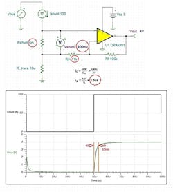
As an alternative, you could cascade two OPA391 stages, each with a gain of 10, but it’s an expensive solution that takes up considerable board space. Another approach is to substitute the OPA392 for the OPA391 in Figure 1. The OPA392’s higher GBW of 13 MHz will result in a tR of 2.7 ms at GCL = 101. The tradeoff here is the OPA392’s higher quiescent current: 1.2 mA vs. 24 µA for the OPA391.
Implementing a TIA
Photodiode-based light sensing is a common op-amp application found in products ranging from medical equipment to point-of-sale (POS) machines. Most applications operate the photodiode in photoconductive mode, with an op amp in a TIA configuration converting the current to a voltage.
To implement a TIA circuit, you can use the precision OPA3S328 dual op amp, which offers a low offset voltage of ±10 µV and a low-input bias current of ±0.2 pA. It also features integrated switches. A version in a QFN package incorporates an integrated 1-to-2 switch matrix and a 1-to-3 switch matrix, while a version in a DSBGA package incorporates two 1-to-3 switch matrices.
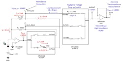
Figure 3 shows an OPA3S328 in a QFN package configured as a programmable gain TIA. It offers the options to switch in either a 200-kΩ or 2-kΩ feedback resistor using the device’s 1-to-2 switch matrix.
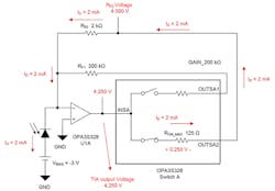
The switch on-resistance varies with voltage and temperature and can produce gain error drift as well as errors related to nonlinearity and distortion, especially with low values of feedback resistors. You can virtually eliminate these errors by using the QFN package’s second switch matrix to establish Kelvin connections directly at the feedback resistors’ terminals (Fig. 4). Then, you can configure the package’s second op amp as a high-impedance buffer, resulting in negligible voltage drop across the second set of switches.
PCB Layout
In addition to contending with parameters such as slew rate and small-signal rise time and circuit configurations such as the TIA, analog-circuit designers face other challenges related to printed-circuit-board layout issues. For an optimum layout, avoid 90-degree angles, keep traces short and wide, and keep components close together. Make connections to the op amp’s inverting pin as short as possible to reduce stray capacitance.
In addition, place decoupling capacitors as close to the op amp’s supply pins as possible. If you’re using multiple decoupling capacitors, place the smallest one nearest the supply pin, and don’t place vias between the decoupling capacitors and the supply pins. Finally, pour at least one solid ground plane.
Conclusion
A thorough understanding of parameters such as gain, GBW, and slew rate can help you quickly design op-amp circuits that measure voltage across a low-side shunt or convert a photodiode’s output current to a voltage. With your circuit design complete, adhere to some basic PCB layout guidelines to ensure a successful end product.
About the Author

Rick Nelson
Contributing Editor
Rick is currently Contributing Technical Editor. He was Executive Editor for EE in 2011-2018. Previously he served on several publications, including EDN and Vision Systems Design, and has received awards for signed editorials from the American Society of Business Publication Editors. He began as a design engineer at General Electric and Litton Industries and earned a BSEE degree from Penn State.
Comment About the Article
To join the conversation, and become an exclusive member of Electronic Design, create an account today!

Leaders relevant to this article: