CTSD Precision ADCs (Part 1): Improving Signal-Chain Design Time
This article is part of the Analog Series: Optimizing Digital Processing with CTSD Precision ADCs
Members can download this article in PDF format.
What you'll learn:
- Why are more precision applications adopting CTSD ADCs?
- How do CTSD ADCs simplify the signal chain?
- Steps for choosing and interfacing with the right ADC.
- CTSD vs. DTSD technology.
In many digital processing applications and algorithms, the demand to have better resolution and precision for all converter technologies has increased over the last two decades. The limited resolution/precision of analog-to-digital converters (ADCs) was enhanced by using an external digital controller that would extract and deliver more precise results using software techniques such as averaging and optimized filtering schemes.
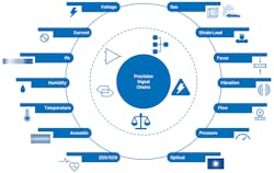
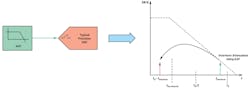
To reduce extensive postprocessing at the digital microcontroller or DSP, designers could use a high-performance precision ADC. This would reduce optimization time at the digital side, and a lower-cost microcontroller or DSP also could be considered. The applications and markets for precision ADCs are widespread (Fig. 1):
- Industrial instrumentation: vibration analysis, temperature/pressure/strain/flow measurements, dynamic signal analysis, acoustic analysis
- Medical instrumentation: electrophysiology, blood analysis, electrocardiogram (EKG/ECG)
- Defense applications: sonar, telemetry
- Test and measurement: audio test, hardware-in-loop, power quality analysis
The analog input signal to be processed by an ADC could be a sensor signal with voltage, current output, or a feedback control-loop signal with bandwidth ranging from dc to a few hundred kilohertz. The ADC digital output format and rate depend on the application and postprocessing required by the following digital controller.
In general, signal-chain designers follow the Nyquist sampling theorem and program the ADC’s output data rate (ODR) for the digital controller to be at least twice the input frequency. Most ADCs provide the flexibility to tune the ODR based on the signal frequency band of interest.
For currently available ADCs, several signal-conditioning stages are involved before the ADC can interact with the input signal. Signal-conditioning circuits with stringent requirements need to be designed and tailored around specific and individual ADC technologies to ensure that ADC datasheet performance can be achieved.
A signal-chain designer’s job doesn’t stop after the selection of the ADC. Considerable time and effort are often required to design and fine-tune this surrounding periphery. Analog Devices provides a high level of technical support in the form of design simulation tools and models to overcome most of these inherent design challenges.
A New Approach: Easing the Design Journey with CTSD Architecture
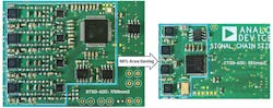
Continuous-time sigma-delta (CTSD) architecture, which has been predominantly used in audio and high-speed ADCs, is being tailored for precision applications to achieve the highest precision while leveraging its unique signal-chain simplification properties. The advantages of this architecture remove the burdens involved with designing the periphery. Figure 2 shows a small snippet of how current ADC signal chains can be simplified and shrunk by 68% using this new solution to enable high channel densities.
To illustrate the simplification that CTSD ADC technology brings to the signal chain, this article highlights some of the key challenges involved in incumbent signal-chain design for general applications. It also shows how CTSD ADCs ease these challenges.
So, let’s start with a few design steps involved in incumbent signal chains, with the very first task being the selection of the right ADC to best fit the targeted application.
Step 1: Selecting the ADC
When selecting from the wide range of available ADCs, important considerations are resolution and accuracy, signal bandwidth, ODR, signal type, and the range to be processed. Generally, in most of the applications, digital controllers require their algorithms to process amplitude, phase, or frequency on the input signal.
To accurately measure any of the previous factors, the errors added in the process of digitization need to be minimal. The major errors and their corresponding measurement terminology are detailed in the table and explained in further detail in the Essential Guide to Data Conversion.
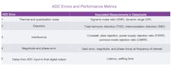
The performance metrics in the table are related to signal amplitude and frequency, and they’re generally termed as ac performance parameters.
For dc or near dc applications, such as power metering, that deal with 50- to 60-Hz input signals, ADC errors like offset, gain, INL, and flicker noise would have to be considered. These dc performance parameters also require a certain level of temperature stability relating to an application’s intended use.
ADI has a wide range of high-performance ADCs to meet system requirements of several applications, be they precision-based, speed-based, or based on a restricted power budget. Just comparing one set of ADC specifications to another isn’t the way to choose an ADC. The overall system performance and design challenges must be considered, and that’s where the choice of ADC technology or architecture comes into play.
Two broad classifications of ADC architectures are traditionally preferred. The most popular is the successive-approximation-register (SAR) ADC, which follows the simple Nyquist theorem. It states that a signal can be reconstructed if sampled at twice its frequency. The advantages of SAR ADCs are excellent dc performance and small form factors with low latency and power consumption scaling with ODR.
The second technology choice is a discrete-time sigma-delta (DTSD) ADC, which works on the principle that the greater the number of samples, lesser is the information lost. So, the sampling frequency is much higher than the stated Nyquist frequency, a scheme referred to as oversampling. An added advantage from this architecture is that the errors added due to sampling are minimized in the frequency band of interest. Because of this, DTSD ADCs have both excellent dc and ac performance but a higher latency.
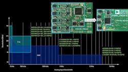
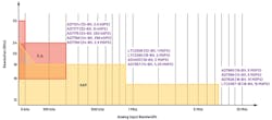
Figure 3 shows an illustration of the typical analog input bandwidths of both SAR and DTSD ADCs, with some popular product choices at various speeds and resolution. The Precision Quick Search feature also can be referenced to help in your choice of ADC.
In addition, a new class of precision ADCs are now available. Based on CTSD ADCs, they’re on par with the performance of DTSD ADCs but are unique with regard to simplifying the entire signal-chain design process. The challenges highlighted in the next few design steps of an incumbent signal chain can be addressed by this new ADC family.
Step 2: Interfacing the Input to the ADC
Sensors whose outputs are to be processed by the ADC may have very high sensitivity. Designers must have a good understanding of the ADC input structure to which the sensor will be interfaced to ensure ADC errors don’t mask or distort the actual sensor signal.
In conventional SAR, DTSD ADCs, the input structure is known as the switched capacitor sample-and-hold circuit (Fig. 4). At every sampling clock edge, when the sample switch changes its ON/OFF state, finite current demand needs to be supported to charge or discharge the hold capacitor to a new sampled input value. This current demand must be supplied by the input source, which, in our case of discussion, is the sensor.
In addition, the switch itself has some on-chip parasitic capacitors that inject some charge back onto the source, which is called charge injection kickback. This added error source also needs to be absorbed by the sensor to avoid corruption of the sensor signal.
Most of the sensors are incapable of providing such a magnitude of currents, indicating that they fall short of driving switching circuitry directly. In a different scenario, say even if a sensor can support these current demands, the sensor’s finite impedance would add an error at the ADC input.
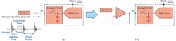
The charge injection current is a function of input; this current causes an input dependent voltage drop across the sensor impedance. As shown in Figure 4a, the input of the ADC is then in error. One solution to solve these issues is to place a driving amplifier between the sensor and ADC (Fig. 4b).
Now we need to set the criteria for this amplifier. First and foremost, the amplifier should support the charging current and absorb the charge injection kickback. Next, this amplifier’s output needs to be fully settled at the end of the sampling edge so that the ADC samples input without added errors. This means the amplifier should have the capability to provide instantaneous current steps that map to having a high slew rate. Further, it should provide a fast settling response to these transient events, which maps to having high bandwidth. As the sampling frequency and resolution of the ADC increases, meeting these requirements becomes critical.
The big challenge for designers, especially those who work with medium-bandwidth applications, is to identify the right amplifier for the ADC. As indicated earlier, ADI provides a set of simulation models and precision ADC driver tools to ease this step, but for a designer, it’s an added design step to achieve the datasheet performance of the ADC.
Some of the new age SAR and DTSD ADCs have mitigated this challenge by using novel sampling techniques to completely reduce the transient current demand, or by having an integrated amplifier. But either solution limits the range of signal bandwidth or penalizes ADC performance.
The CTSD ADC advantage: CTSD ADCs address this challenge by providing an easy-to-drive resistive input instead of a switched capacitor input. This shows that there are no hard requirements of high-bandwidth, large-slew-rate amplifiers. If sensors can directly drive this resistive load, they can be directly interfaced to a CTSD ADC. Otherwise, any low-bandwidth, low-noise amplifier could be interfaced between a sensor and a CTSD ADC.
Step 3: Interfacing the Reference to the ADC
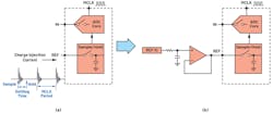
The challenge involved with interfacing to a reference is similar to input interfacing. The reference input for conventional ADCs also is a switched capacitor. At every sampling clock edge, the reference source needs to charge the internal capacitors, thus demanding large switching current with good settling time.
The reference ICs available can’t support large switching current demand and have limited bandwidth. The second interfacing challenge is that noise from these references is large in comparison to an ADC’s noise. To filter this noise, a first-order RC circuit is used.
On one hand, we’re band-limiting the reference for noise, while on the other hand, we’re demanding fast settling time. These are two opposing requirements to satisfy. For this reason, a low-noise buffer is used to drive the ADC reference pin (Fig. 5b). Based on the sampling frequency and resolution of an ADC, the slew rate and bandwidth of this buffer is decided.
Again, like with our precision input driver tools, ADI has tools to simulate and select the correct reference buffers for an ADC. And similar to input, some of the new age SAR and DTSD ADCs also have the option of an integrated reference buffer, but they come with performance and bandwidth limitations.
The CTSD ADC advantage: This design step can be completely skipped by using a CTSD ADC. It provides a new, easy option for driving a resistive load that doesn’t require such a high-bandwidth, large-slew-rate buffer. The reference IC with low-pass filter can be directly interfaced to the reference pin.
Step 4: Making a Signal Chain Immune to Interference
Sampling and digitizing a continuous signal causes loss of information, which is termed as quantization noise. The sampling frequency and number of bits set the performance limit for an ADC architecture.
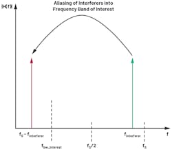
After addressing the performance and interfacing challenges for the reference and input, the next struggle is to address the issue of high-frequency (HF) interferers/noise folding into the low-frequency bandwidth of interest. This is termed aliasing or folding back. These reflected images of the HF or out-of-band interferers into the bandwidth of interest cause signal-to-noise ratio (SNR) degradation.
Citing the sampling theorem, any tone around the sampling frequency folds back in-band (Fig. 6), which causes an unwanted information or error in the frequency band of interest. Further details on aliasing can be found in the tutorial MT-002: What the Nyquist Criterion Means to Your Sampled Data System Design.
To mitigate the effect of foldback, one solution is to use a type of low-pass filter known as an antialiasing filter (AAF). It attenuates the unwanted interferer’s magnitude such that when this attenuated interferer folds back in-band, the desired SNR is maintained. This low-pass filter is generally incorporated with a driver amplifier (Fig. 7).
When designing this amplifier, the biggest challenge is finding a balance between faster settling and the low-pass filtering requirements. An added challenge is that this solution must be fine-tuned for each application requirement, which limits the adoption of single platform design across various applications. ADI has many antialiasing filter tool designs to help designers overcome this challenge.
The CTSD ADC advantage: This immunity to interference is addressed by the inherent alias rejection property of the CTSD ADC itself, a feature that’s unique only to CTSD ADCs. The AAF isn’t required for ADCs with this technology. Therefore, we would be one step nearer to directly interfacing a CTSD ADC to a sensor without much effort.
Step 5: Selecting the ADC Clock Frequency and the Output Data Rate
Next, let’s discuss the clock requirements for the two classes of traditional ADCs covered earlier (Fig. 8). The DTSD is an oversampled ADC, which means that the ADC is sampled at a higher-than-Nyquist sampling rate. But giving ADC oversampled data directly to the external digital controller implies we’re overloading it with lots of redundant information. In an oversampled system, the core ADC output is decimated using on-chip digital filters that enable the final ADC digital output at a lower data rate, which is usually twice the signal frequency.
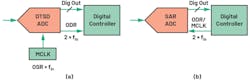
For DTSD ADCs, the designer needs to plan for the provision of the high-frequency sampling clock for the core ADC and program the desired output data rate. The ADC will give a final digital output at this desired ODR and the ODR clock. A digital controller uses this ODR clock to clock in the data.
Next, we address the clock requirements of SAR ADCs, which usually follow the Nyquist theorem. Here, the sampling clock of the ADC is provided by a digital controller; the clock also acts as an ODR. But there’s less flexibility in the timing of this clock—the sample-and-hold timing needs to be well-controlled to get optimum performance from the ADC, which also indicates that the timing of the digital output needs to be well-aligned with these requirements.
In understanding the clock requirements of both architectures, we see that the ODR is coupled to the sampling clock of the ADC. This is a limitation in many systems where ODR can drift or change dynamically, or needs to be tuned to the analog input signal frequency.
The CTSD ADC advantage: The CTSD ADC couples with a novel asynchronous-sample-rate converter (ASRC) that resamples the core ADC data at any desired ODR. The ASRC also enables designers to granularly set the ODR at any frequency and go beyond the age-old restriction of limiting ODR to a multiple of sampling frequency. The frequency and timing requirements of ODR are now purely a function of the digital interface and completely decoupled from the ADC sampling frequency. This feature eases digital isolation design for signal-chain designers.
Step 6: Interfacing with the External Digital Controller
Traditionally, there are two types of data interface modes for ADCs to communicate with the digital controller. One involves the ADC acting as a host, providing the digital/ODR clock, and deciding on the clock’s edges for the digital controller to clock-in the ADC data. The other type is hosted mode (receiver mode), in which the digital controller is the host, provides the ODR clock, and decides the clock edges at which the ADC data will be clocked in.
Continuing from Step 5, if a designer selects a DTSD ADC, the ADC acts as host for the following digital controller since the ADC provides the ODR clock. If a SAR ADC is selected, the digital controller needs to provide the ODR clock, implying SAR ADCs are always configured as hosted peripheral. So, the obvious limitation is that, once an ADC architecture is chosen, the digital interface is restricted to being in host mode or hosted mode. Currently, there’s no flexibility in choosing the interface regardless of ADC architecture.
The CTSD ADC advantage: The novel ASRC that’s been coupled with a CTSD ADC enables designers to independently configure the ADC data interface mode. This opens up a whole new opportunity for applications where high-performing ADCs can be configured in any mode suitable for the digital controller of the application irrespective of ADC architecture.
Putting It All Together
Figure 9 shows the building blocks of a traditional signal chain with an analog front end (AFE) comprising an ADC input driver, an alias rejection filter, and a reference buffer that can be drastically simplified by a CTSD ADC. Figure 10a illustrates an example signal chain with a DTSD ADC that requires significant design effort to fine-tune and derive the datasheet performance of the ADC. To ease the customer journey, ADI has reference designs that can be reused or retweaked for various applications for these ADCs.
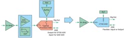
Figure 10b shows a signal chain with a CTSD ADC and its simplified AFE because its ADC core doesn’t have a switch capacitor sampler at the input and reference. The switch sampler is moved to a later stage of the ADC core, making the signal input and reference input purely resistive. This results in an almost nonsampling ADC, making it a class of its own.
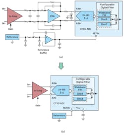
Also, the signal transfer function of this class of ADCs mimics the antialiasing filter response, which means it inherently attenuates noise interferers. With CTSD technology, the ADC is reduced to an easy plug-and-play component.
In summary, CTSD ADCs simplify signal-chain design while achieving a system solution with the same performance level as a traditional ADC signal chain, along with offering the following advantages:
- Provides alias-free, low-latency signal chain with excellent channel-to-channel phase matching.
- Simplifies the analog front end with no added step of selection and fine-tuning of high bandwidth input and reference driver buffers, enabling higher channel density.
- Breaks barrier of ODR being a function of the sampling clock.
- Gives independent control of interface to external digital controller.
- Improves the signal-chain reliability rating, which is a direct result of periphery component reduction.
- Shrinks size and has a 68% reduction in BOM, leading to faster time to market for customers.
The next few articles in this series will explain the concepts of CTSD ADCs and ASRCs in greater detail, highlight the signal-chain advantages, and will conclude with leveraging the features of the new AD7134. Keep a look out to learn more about the breakthrough CTSD and ASRC technologies that can simplify your designs!
Acknowledgements
The authors would like to thank product applications engineer Naiqian Ren and product marketing engineer Mark Murphy for their useful insights in writing this article.
Read more articles in the Analog Series: Optimizing Digital Processing with CTSD Precision ADCs
References
“Application Note AN-282: Fundamentals of Sampled Data Systems.” Analog Devices, Inc.
Driving Precision Converters: Selecting Voltage References and Amplifiers. Analog Devices, Inc.
Kester, Walt. “MT-021 Tutorial: ADC Architectures II: Successive Approximation ADCs.” Analog Devices, Inc., 2009.
Sigma-Delta ADC Tutorial. Analog Devices, Inc.
Shaikh, Wasim and Srikanth Nittala. “AC and DC Data Acquisition Signal Chains Made Easy.” Analog Dialogue, Vol. 54, No. 3, August 2020.
About the Author
Abhilasha Kawle
Senior Analog Design Engineer, Analog Devices
Abhilasha Kawle is a senior analog design engineer at Analog Devices in the Linear and Precision Technology Group based in Bangalore, India. She graduated in 2007 from Indian Institute of Science, Bangalore, with a master’s degree in electronic design and technology.
Comment About the Article
To join the conversation, and become an exclusive member of Electronic Design, create an account today!

Leaders relevant to this article: