CTSD Precision ADCs (Part 2): CTSD Architecture Explained
This article is part of the Analog Series: Optimizing Digital Processing with CTSD Precision ADCs
Members can download this article in PDF format.
What you'll learn:
- Step-by-step approach to building a CTSD modulator loop.
- Introducing the analog accumulator.
- A closer look at oversampling and noise shaping.
- The clock sensitivity of CTSD ADCs.
In Part 1, we highlighted the key challenges of incumbent signal-chain designs that can be simplified significantly with a precision continuous-time sigma-delta (CTSD) ADC, as it maintains continuous-time signal integrity while achieving the highest precision. Now, the question is what’s behind the CTSD architecture that enables it to achieve these advantages?
The traditional approach of explaining the concept of CTSD technology is to first gain an understanding of the basics of a discrete-time sigma-delta (DTSD) modulator loop and then substituting the discrete-time loop elements with equivalent continuous-time elements. While this method provides in-depth insight of sigma-delta functionality, we aim to provide a more intuitive understanding behind the inherent advantages of precision CTSD ADCs.
To begin, we will outline a step-by-step approach to building a CTSD modulator loop starting with the widely known, closed-loop inverting amplifier configuration and combining it with an ADC and a DAC. Then we’ll evaluate the basic sigma-delta functionality from the circuit we build.
Step 1: Revisiting the Closed-Loop Inverting-Amplifier Configuration
One of the key advantages of the CTSD ADC is that it offers an easy-to-drive continuous resistive input rather than a traditional switched capacitor sampler upfront. One of the circuits that has a similar input impedance concept is the inverting amplifier, which we will use as a starting block toward building a CTSD modulator loop.
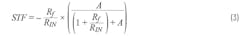
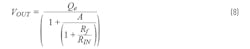
A closed-loop op-amp configuration has always been the go-to option for replicating an analog input with high fidelity. Figure 1 shows one of the most popular op-amp configurations, which is called an inverting amplifier configuration.1 One of the measures of the fidelity is the output to input gain, also known as—in sigma-delta nomenclature—the signal transfer function (STF). Determining the parameters that affect the STF requires analyzing the circuit.
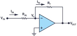
To refresh our mathematical skills, let’s revisit the derivation of the famous VOUT/VIN. In the first step, the open-loop gain of op amp A is assumed to be infinite. This assumption directly leads to making the op amp’s input negative (Vn) at potential ground. The application of Kirchhoff’s laws at this node gives:


From here, textbooks generally describe the sensitivity toward the RIN, Rf, and A parameters. For our case, lets proceed toward building the CTSD loop.
Step 2: Introducing Discretization into the Amplifier
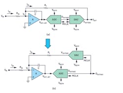
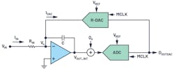
The requirement for our ADC signal chain is a digitized version of VIN. In our next step, we introduce the digitization in this circuit. Rather than use the traditional way of putting a sampling ADC directly at the input signal, we’ll try a different approach and put a representative ADC that follows the amplifier output to obtain the digitized data. But the output of the ADC can’t be used as feedback directly—it’s required to be an analog voltage. So, then, we need to follow up the ADC with a voltage digital-to-analog converter (DAC) (Fig. 2).
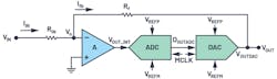
Because of the ADC and DAC, VOUT is still a representation of VIN, but with quantization error due to the added digitization. Therefore, nothing has changed in the signal flow from VIN to VOUT. One point of note here: Keep the functionality of the loop symmetric to about 0 V; easing our mathematical derivation, the references of ADC and DAC are chosen to be:

Step 3: Introducing the Analog Accumulator—the Integrator
Is the closed-loop configuration in Figure 2 stable? Both the ADC and DAC are discretization elements working on a sampling clock (MCLK). It’s been an unachievable dream of converter specialists to design a delay-free ADC or DAC. Since these loop elements are clocked, the input is generally sampled on one edge and processed on the other clock edge. Thus, the output of the ADC and DAC combination VOUT, which is the feedback in Figure 2, is available only after one clock cycle delay.
Does this delay in feedback have any implication on stability? Let’s trace how VIN transfers along. For simplification, let’s assume VIN = 1, RIN = 1, Rf = 1, and the gain of op amp A is 100. At the first clock cycle, the input voltage is 1 and the DAC output feedback, VOUT or VOUTDAC, is 0 and not available until the next clock edge (see table).

As we trace the error between the input and feedback to the output of the amplifier and ADC, we can see the output keeps growing exponentially. This is technically termed as the runaway problem.
This happened because the ADC input works on instantaneous error gained up by the amplifier, i.e., the ADC decides even before the feedback is available, which wasn’t required. If the ADC works on an accumulated, averaged error data so that the error due to one clock delay of feedback is averaged out, then the output of system would be bounded.
The integrator is one such analog equivalent of an averaging accumulator. The gain of the loop is still high but only at low frequencies, or, in other words, in the frequency bandwidth of interest. This ensures that the ADC isn’t presented with any instantaneous errors that can lead to a runaway situation. So, the loop is now an amplifier modified as an integrator followed by the ADC and DAC (Fig. 3a).
Step 4: Simplifying the Feedback Resistor
Our element of interest is DOUTADC, so let’s rearrange the loop elements to highlight DOUTADC as the output of the system (Fig. 3b). Next, let’s visit the simplification of the DAC and Rf path, and for that let’s dig into the DAC’s details.
The purpose of the DAC is to convert a digital code (DIN) to an equivalent analog current or voltage in proportion to the reference. To further extend the advantages of continuity to reference, what we’ve considered here is a general DAC architecture based on a resistor ladder that has no switching load on reference.
Let’s review a thermometric resistor DAC,2 which converts DIN to the DAC current, with relation to Equation 5:

where VREF = VREFP – VREFM, the total reference voltage across the DAC.
- DIN = Digital input in the thermometric code
- Rf = Feedback resistor; split as each unit element
- N = Number of bits
To get the voltage output, an I to V conversion follows by using an op amp in a transimpedance configuration,3 as shown in Figure 4.
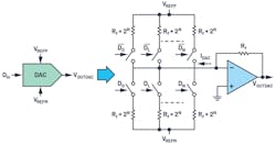
Therefore:

Going back to our discretized loop of Figure 3b, this VOUTDAC is again converted back to current, Ifb, through the feedback resistor of the inverting amplifier, implying the signal flow is IDAC → VOUTDA C → Ifb. Mathematically:

From the above signal flow and formula, we see that converting VOUTDAC to Ifb is a redundant step that can be bypassed. Removing the redundant elements and, for simplicity, representing (VREFP – VREFM) as VREF, let’s redraw our loop (Fig. 5).
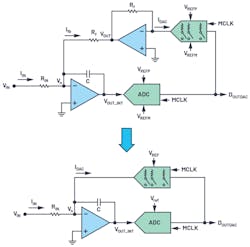
And voilà! We’ve built a first-order sigma-delta loop! And all by stitching together well-known elements—an inverting amplifier, an ADC, and a DAC.
Step 5: Understanding Oversampling
Up to now, we’ve grasped the construction of a CTSD loop, but not yet appreciated the particularities offered by this fanciful loop. The first step toward that is understanding oversampling. ADC data is useful only if there are enough sampled and digitized data points to extract or interpret the analog signal information.
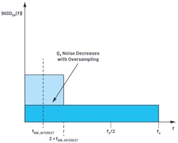
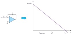
The Nyquist theorem advises that, for faithful reconstruction of an input signal, the sampling frequency of the ADC should be at least twice the frequency of the signal. If we keep adding more data points over this minimum requirement, it would further reduce the error in interpretation.
Following that line of thought, in sigma-delta, the sampling frequency is selected to be much higher than the suggested Nyquist frequency. This is known as oversampling. Oversampling4 helps reduce the quantization noise in the frequency band of interest by spreading the total noise over much higher frequency (Fig. 6).
Step 6: Understanding Noise Shaping
Signal-chain designers shouldn’t feel lost when sigma-delta experts use terms like noise transfer function (NTF) or noise shaping.4 Our next step will help them get an intuitive understanding of these terms, as they’re unique to sigma-delta converter nomenclature. Let’s revisit our simple inverting amplifier configuration and introduce the error Qe at the output of the amplifier (Fig. 7).
The contribution of this error at the output is quantified as:
The mathematical formula translates that the error Qe is attenuated by the open-loop gain of the amplifier, which is just reiterating the advantage of a closed loop.
This understanding of the closed-loop advantage can be extended to quantization error Qe of the ADC in the CTSD loop. This is the error introduced due to digitization of the continuous signal at the output of the integrator (Fig. 8).
We can now intuitively conclude that this Qe would be attenuated by the integrator. The integrator TF is |HINTEG (f)| = 1/|s × RC| = 1/2πfRC, and its corresponding frequency domain representation is shown in Figure 9. Its profile is equivalent to a low-pass filter profile with high gain at low frequencies, and the gain reduces linearly as frequency increases. Correspondingly, the attenuation for Qe would then look like a high-pass filter.
The mathematical representation of this attenuation factor is the noise transfer function. For an interim, let’s ignore the sampler in the ADC and the switches in the DAC. The NTF, VOUTADC ⁄ Qe, can be evaluated by following the same exercise as we did for the inverting amplifier configuration, which in the frequency domain looks like a high-pass filter profile (Fig. 10):

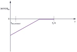
In the frequency band of interest, the quantization noise is completely attenuated and pushed to “not to our concern” high frequencies. This is what’s called noise shaping.
With the sampler in loop, the quantization-noise-shaping analogy remains the same. The difference being the NTF frequency response would have replicated images at every multiple of fS (Fig. 10, again), thus creating notches at every integer multiple of the sampling frequency.
The uniqueness of sigma-delta architecture lies in the fact that putting an integrator and a DAC loop around a crude ADC—for example, a 4-bit ADC—and applying the concept of oversampling and noise shaping reduces the quantization noise significantly in the frequency bandwidth of interest. It also masks this crude ADC to a 16- to 24-bit precision ADC.
These basics of the first-order CTSD ADC can now be extended to any order of modulator loop. The sampling frequency, the crude ADC specifications, and the order of loop are top-level design decisions driven by the performance requirements of the ADC.
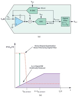
Step 7: Completing the CTSD Modulator with a Digital Filter
Generally, in an ADC signal chain, the digitized data is post-processed by an external digital controller for any signal information extraction. In sigma-delta architecture, as we know now, the signal is oversampled. If this oversampled digital data is directly given to the external controller, then a lot of redundant data needs to be processed. This causes excess power and real-estate cost overheads in the digital controller design.
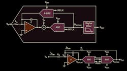
Therefore, before data is presented to the digital controller, the data samples are dropped in an efficient way without affecting the performance. This process, called decimation, is done by digital decimation filters. Figure 11 shows a typical CTSD modulator with on-chip digital decimation filters.
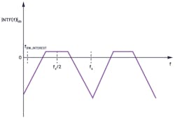
Figure 12b shows frequency response for an in-band analog input signal. At the output of the modulator, we observe the noise shaping of the quantization noise, drastically reducing it in the frequency band of interest. The digital filter helps attenuate the shaped noise beyond this frequency bandwidth of interest so that the final digital output (DOUT) is at the Nyquist sampling rate.
Step 8: Understanding the Clock Sensitivity of CTSD ADCs
So far, we have understood how CTSD ADCs keep the continuous integrity of the input signal, which significantly simplifies signal-chain design. This architecture also has a few limitations, mainly dealing with the sampling clock MCLK.
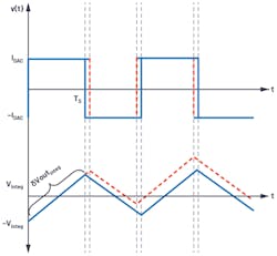
The CTSD modulator loop works on the concept of integrating the error current between IIN and IDAC. Any error in this integrated value would cause the ADC in loop to sample the error and reflect this in the output. For our first-order integrator loop, the integrated value over the sampling time period of Ts for constant IIN and IDAC is given by:

For an input of 0, the parameters that would affect this integration error are:
- MCLK frequency: As indicated by Equation 10, if the MCLK frequency scales, then the RC coefficient that controls the slope of integration also needs to be retuned to get back the same integrated value. This implies that a CTSD modulator is tuned for a fixed MCLK clock frequency and can’t support varying MCLK.
- MCLK jitter: The DAC code and, hence, IDAC change every clock time period Ts. If the IDAC time period randomly changes, then the average integrated value keeps changing, as shown in Figure 13. So, any error in the sampling clock time period in the form of jitter would affect the modulator loop’s performance.
CTSD ADCs are sensitive to the frequency and jitter of an MCLK because of the above reasons.5 But Analog Devices has identified solutions to work around these fallacies. For example, the challenges of generating and routing accurate, low-jitter MCLK along the system to the ADC can be addressed using a local, low-cost crystal and oscillator near the ADC.
The fallacy around the fixed sampling frequency has been addressed by using asynchronous sample-rate conversion (ASRC) that enables a variable and independent digital output data rate for the digital controller irrespective of the fixed sampling MCLK. More information about this will be detailed later in this series.
Step 9: All Set to Explain the CTSD Concept to Your Buddies!
Part 1 of the series highlighted certain signal-chain advantages of a CTSD ADC, while this article focused on the insights of the modulator loop built from Step 1 to Step 6 using the concept of a closed-loop op-amp configuration. Figure 12a also helped us visualize these advantages.
The input impedance of a CTSD ADC is equivalent to the input impedance of the inverting amplifier, which is resistive and easy to drive. Using innovative techniques, the reference used by the modulator loop’s DAC also has been made resistive. The sampler of the ADC is after the integrator and not directly at the input, which enables inherent alias rejection for interferers outside the frequency band of interest.
We will deep dive into each of these advantages and their corresponding impact in a signal chain in the following articles in this series. Keep an eye out for Part 3—it focuses on inherent alias rejection and its quantification using a set of measurements and performance parameters introduced for the first time with the AD4134, which is based on the CTSD architecture.
Acknowledgements
The author would like to thank Praveen Varma and Roberto Maurino for their helpful insights in putting together this simplified way of explaining the CTSD ADC technology.
Read more articles in the Analog Series: Optimizing Digital Processing with CTSD Precision ADCs
References
1. Hank Zumbahlen. “Mini Tutorial MT-213: Inverting Amplifier.” Analog Devices, Inc., February 2013.
2. Walt Kester. “MT-014 Tutorial: Basic DAC Architectures I: String DACs and Thermometer (Fully Decoded) DACs.” Analog Devices, Inc., 2009.
3. Luis Orozco. “Programmable-Gain Transimpedance Amplifiers Maximize Dynamic Range in Spectroscopy Systems.” Analog Dialogue, Vol. 47, No. 2, May 2013.
4. Walt Kester. “MT-022 Tutorial: ADC Architectures III: Sigma-Delta ADC Basics.” Analog Devices, Inc., 2009.
5. Pawel Czapor. “Sigma-Delta ADC Clocking—More Than Jitter.” Analog Dialogue, Vol. 53, No. 3, April 2019.
Pavan, Shanthi, Richard Schreier, and Gabor C. Temes. Understanding Delta-Sigma Data Converters, 2nd edition. Wiley, January 2017.
About the Author
Abhilasha Kawle
Senior Analog Design Engineer, Analog Devices
Abhilasha Kawle is a senior analog design engineer at Analog Devices in the Linear and Precision Technology Group based in Bangalore, India. She graduated in 2007 from Indian Institute of Science, Bangalore, with a master’s degree in electronic design and technology.
Comment About the Article
To join the conversation, and become an exclusive member of Electronic Design, create an account today!

Leaders relevant to this article: