Tiny Dual Op Amp Features Low Offsets, 20-MHz Bandwidth
Given the countless number of operational-amplifier (op amp) makes and models already on the market, it might seem that there’s little call for yet another one. After all, unlike high-level multifunction ICs with many internal blocks, these humble building blocks implement just a single function, admittedly one that can be configured for many applications.
Nonetheless, the reality is that vendors are still introducing new op amps, each being a classic case study in balancing multiple tradeoffs such as power, offset voltage, bias current, distortion, overload characters, and more.
The simple op amp has an impressive array of defining parameters of differing interest for various applications. Some op amps excel at one or two specifications but are only so-so at others. Other op amps are very good across many of these specifications but don’t excel at any single one, and thus are well-suited for some situations.
ST’s New Dual Op Amp
A recent entry into the op-amp market is the TSV772 from STMicroelectronics. The dual op amp combines high accuracy, low power consumption, and multiple package options that includes an extremely small 2.0- × 2.0-mm DFN8 package.
Extending an existing high-performance 5-V op-amp family, the TSV772 can operate from a 2.0- to 5.5-V single supply, has rail-to-rail inputs and outputs, 20-MHz gain-bandwidth (GBW), and is unity-gain stable. A slew rate of 13 V/µs, input noise density of 7 nV/√Hz, and 4-kV ESD capability (human body model, or HBM) enhances the TSV772’s accuracy of associated measurements since it’s virtually unaffected by noise or input bias current.
The dual device is characterized for an output capacitive load of 47 pF, simplifying its use as an analog-to-digital converter (ADC) input buffer. The maximum input-offset voltage of 200 µV (at 25°C) ensures accurate handling of low-amplitude signals. The inherent accuracy also saves on the need for expensive, precision external resistors and helps avoid trimming or calibrating circuits in production.
Moreover, the TSV772 is well-suited for applications such as amplifying the low current output of photodiodes in smoke detectors and even outputs of medical sensors. Other applications include high-bandwidth, low- and high-side current sensing (it’s optimized for low-side current sensing and trimmed for a common-mode voltage close to ground), and active filters. Its performance also enables accurate current measurement critical to the sensing starting point for efficient power conversion in solar generators, telecom infrastructure equipment, and computer servers.
Application Examples
The 30-page datasheet provides minimum, maximum, and typical specifications for many parameters, as well as tables and graphs of performance across various perspectives and temperature, as op amp users expect.
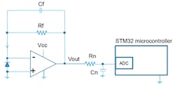
It also provides some basic application-circuit examples such as the photodiode transimpedance-amplifier circuit (Fig. 1). Here, the op amp is the core of a front-end transimpedance-amplifier that converts the tiny photodiode output current in the nanoamp range into a voltage for the circuit (which may include the ADC, but it’s not mandatory),with Vout = Rf × Iphotodiode.
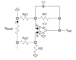
Another application is low-side current sensing—usually somewhat easier to implement than its complement of high-side sensing. In this case, the sense resistor Rshunt is located between the load and the circuit ground, and the resultant voltage drop is amplified using the op amp (Fig. 2).
In the usual arrangement with resistor-pair values chosen selected to be equal:
Rf2 = Rf1 = Rf and Rg2 = Rg1 = Rg
the complicated shunt-current versus output-voltage equation simplifies to:
Vout = [Rshunt × I × (Rf/Rg)] − [Vio × (1 + Rf/Rg) + (Rf × Iio)]
where Vio and Iio are the input offset voltage and input offset current, respectively, and which clearly shows the importance of low offset values in this application.
For the a given current value and desired accuracy, the shunt resistor can be chosen to have a lower value. This leads to lower power dissipation, lower voltage drop in the ground path, and lower cost.
The TSV772 dual op amp is available in SO-8 and MiniSO-8 packages, as well as the miniature DFN8 package. Although many of the target applications are in relatively benign settings, −40 to +125°C AEC-Q100 automotive-qualified versions are undergoing certification. Prices start from $0.73 for orders of 1,000 units.
Reference
STMicroelectronics, AN4451, “Signal conditioning for a UV sensor”
About the Author

Bill Schweber
Contributing Editor
Bill Schweber is an electronics engineer who has written three textbooks on electronic communications systems, as well as hundreds of technical articles, opinion columns, and product features. In past roles, he worked as a technical website manager for multiple topic-specific sites for EE Times, as well as both the Executive Editor and Analog Editor at EDN.
At Analog Devices Inc., Bill was in marketing communications (public relations). As a result, he has been on both sides of the technical PR function, presenting company products, stories, and messages to the media and also as the recipient of these.
Prior to the MarCom role at Analog, Bill was associate editor of their respected technical journal and worked in their product marketing and applications engineering groups. Before those roles, he was at Instron Corp., doing hands-on analog- and power-circuit design and systems integration for materials-testing machine controls.
Bill has an MSEE (Univ. of Mass) and BSEE (Columbia Univ.), is a Registered Professional Engineer, and holds an Advanced Class amateur radio license. He has also planned, written, and presented online courses on a variety of engineering topics, including MOSFET basics, ADC selection, and driving LEDs.


