Overcome the Challenges of Using Sub-Milliohm SMD Chip Resistors (Part 1)
This article is part of the Overcome the Challenges of Using Sub-Milliohm SMD Chip Resistors series.
Members can download this article in PDF format.
What you’ll learn:
- How to treat sub-milliohm chips as a separate class of component.
- Strategies to avoid pitfalls during component selection and PCB layout design.
- Uncover opportunities to quantify and minimize error and variation at every stage.
The simplest and most cost-effective way of converting a measured current to a voltage signal is to use a low-ohmic-value current-sense resistor. The upswing in products containing batteries, motors, or actuators that call for current monitoring or control has led to huge market growth for current-sense chip resistors with values below one ohm over the last two decades.
More recently, though, driven by power-efficiency demands and enabled by low-noise voltage-sense amplifiers, the value range has extended downward from milliohms to hundreds of microhms. Such low ohmic values present challenges to the user at many stages in their design and manufacturing processes.
This two-part series considers the nature of these challenges and suggests strategies to overcome them at various stages, including component selection, PCB layout design, verification of the ohmic value of unmounted components, and critical assembly processes. Each stage features potential pitfalls but also opportunities to quantify and minimize error and variation.
Although sub-milliohm chip resistors are still just chip resistors, ideal design strategies treat them as a separate class of component, embracing considerations and techniques that enable their successful use.
Component Selection
Termination Styles
When restricting the temperature sensitivity of a resistor-based current-sensing circuit, it’s well-known that the total terminal resistance from copper, common to both the current-carrying circuit and the voltage-sense circuit, must be restricted as well. That’s because this element of the total measured resistance has a temperature coefficient of resistance (TCR) of +3900 ppm/°C, which contributes to the total TCR in proportion to the resistance ratio.
For example, a total terminal resistance of 100 µΩ, i.e., 50 µΩ at each end, for a 1-mΩ resistor contributes 100 µΩ/1000 µΩ × 3900 ppm/°C = 390 ppm/°C to the TCR. This contrasts with the TCR of the resistance element itself, which is typically better than ±30 ppm/°C. Such separation between the current-carrying and voltage-sense circuits is referred to as a Kelvin connection, an issue that becomes clearly more important as the nominal ohmic value is reduced.
There’s a spectrum of termination styles to address this problem. The most common is the Kelvin connectable two-terminal resistor (Fig. 1a). While this is often the lowest-cost option, it places the onus on the PCB designer to realize a Kelvin connection in the PCB track layout (later we’ll look in detail at how this may best be achieved). Such a component must have a low termination resistance since the Kelvin connection strategy necessarily ends at the surface of the termination.
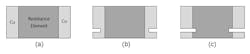
Figure 1b shows an intermediate component type where four solder terminals are provided, but the separation of circuits doesn’t extend all the way into the resistor element. Figure 1c shows a true Kelvin format where there’s no current-carrying termination whatsoever within the voltage-sense circuit. The latter two types offer error-proof PCB layout design and the lowest achievable magnitude of TCR, but generally it comes at a higher cost.
Element Materials
Low-value resistors can be made from both thick- and thin-film materials, but the lowest values available in these technologies are in the multiple-milliohm range. Both types are relatively susceptible to damage from high-current surges. In the case of thick-film technology, the lowest values are associated with high TCR values of several hundred ppm/°C and thus are suited only to low precision use.
For these reasons, most current-sense chip resistors are based on a bulk metal element. This may be either a foil supported on a substrate or a self-supporting metal element. Though the former option allows for the use of thin metal layers to achieve higher values, the latter lends itself to sub-milliohm values.
A range of alloys, each with differing resistivities, are selected by device designers to provide the required ohmic value within the dimensional constraints of the product. From the point of view of the user, the material choice is often unimportant, but there are two exceptions: one is the control of thermally generated errors, and the other is application for non-dc circuits.
A copper-terminated metal-element chip resistor contains at least two boundaries between dissimilar metals. These act as thermocouples and generate a thermoelectric voltage in the presence of a temperature gradient. Furthermore, they’re connected in series, and because of the component’s symmetry, they’re of opposite polarity when the resistor element itself is the main heat source. As a result, if the temperature distribution across the chip resistor is symmetrical, any generated thermoelectric voltages will be cancelled out.
Figure 2a illustrates this balanced state in which the thermal voltages V1 and V2 are equal. Figures 2b and 2c show an example of imbalance due to the external influence of a heat source and a heatsink, respectively. This would lead to a finite value of V1 − V2, which would sum with the measured sense voltage and create a source of error.
In many designs, it’s simply not possible to guarantee thermal symmetry under all operating conditions. In such a case, a chosen part should employ a resistance alloy with a low thermoelectric voltage against copper. These alloys contain manganese in a copper nickel alloy in which the proportion of copper exceeds 80%. The thermoelectric voltages generated across a junction with copper can be as low as 3 µV/°C, which is an order of magnitude lower than for a copper nickel alloy.
The second application-specific driver for resistance alloy selection is the need to avoid iron-bearing alloys in circuits where ac or rapid step changes in dc need to be tracked accurately, as this is not possible with ferromagnetic alloys.
Thermal Design Format
An inherent problem with resistive current sensing is heat, generated at a rate proportional to the square of the current. This may need to be restricted for one of two reasons. First, the design must reduce the effect of temperature increase on the linearity of the component, which can stem from TCR or from thermoelectric voltage errors. Second, it’s necessary to avoid overheating the resistance alloy, which can lead to irreversible ohmic-value change.
This consideration calls for careful thermal design of the assembly. It begins at the component selection stage in response to the basic decision as to where the heat generated should be dissipated; for example, in the air or in the copper PCB tracks. The answer to this depends on the overall thermal-management strategy.
A well-ventilated assembly—with either a high thermal loading already on the PCB or with temperature-sensitive components—would benefit from a resistor that dissipates heat into the air. Conversely, a PCB that’s heatsinked, or has no excess of heat generation and no temperature-sensitive parts, can employ a resistor which dissipates heat mainly to the PCB tracks.
An example of a primarily air-dissipating open-air format is shown in Figure 3a. This can sustain a temperature rise of the hotspot above the solder joints well in excess of 100°C. Its flexible nature makes it virtually immune to temperature cycling or board flex stresses on the solder joints. An example of the primarily PCB dissipating flat-chip format is shown in Figure 3b. The design benefits from its low profile and is generally the lower-cost option.
Most Common Type
After considering the many options of termination style, element material, and thermal design format, the most common type of sub-milliohm resistor is a two-terminal metal-element chip resistor. This resistor type will be considered hereafter in this article.
PCB Layout Design
Near-Kelvin Connection
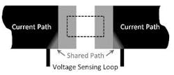
The PCB layout design around a very-low-value resistor is critical to its performance. The most important aspect of this design is the fact that four rather than two tracks must be provided to form a Kelvin connection, even where the component itself has only two terminals.
The aim is to minimize the conductive path shared between the current path and the voltage-sensing loop (Fig. 4), which would increase both the effective ohmic value and the TCR of the mounted part. This may be achieved by connecting the voltage-sense tracks to the inner edges of the solder pads (Fig. 5).
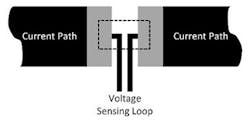
Designers also can take this a step further and split the voltage-sense pads from the current-path pads, so that the solder joints themselves are removed from the shared path, too (Fig. 6). By using this method, it’s possible to approach the accuracy obtained from a true four-terminal resistor.
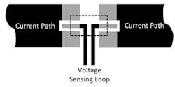
Furthermore, a study1 by Analog Devices based on TT Electronics’ ULR3 0.5-mΩ mounting-pad options has shown that a mounted value tolerance close to 1% may be achieved on a 1% tolerance component. This indicates low additional error due to mounting effects, using a centralized, isolated sense-pad design similar to that of Figure 4c.
Minimization of Sense-Loop Area
A source of error involving high currents that are ac or changing dc is due to the voltage-sensing loop linking with changing magnetic fields. This can induce a noise signal superimposed on the desired voltage sense signal.
To reduce the noise, the loop area contained within the sense resistor, the two voltage-sense tracks, and the sense circuit input should be minimized. This means keeping the sense circuitry as close as possible to the sense resistor and running the voltage-sense tracks close to each other.
A good way to keep these tracks very close is to superimpose them in different PCB layers. Where long track runs are unavoidable, it’s also possible to use periodic vias to cross over the tracks into alternate layers. On a PCB, this replicates the effect of a twisted-pair cable, which, by means of cancellation of induced voltages, allows the circuit to withstand the effect of any changing magnetic fields that have small variations across the spatial periodicity of the twisting.
Connecting Multiple Resistors in Parallel
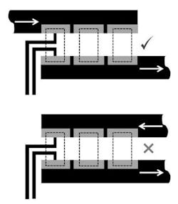
Sometimes, designers are forced to use more than one current-sense resistor connected in parallel, either to meet a high power or surge rating, or to achieve an ohmic value lower than the minimum available. This is problematic but possible. Resistors may be connected in parallel with voltage-sense connections made to just one of the resistors, provided the track layout ensures equal distribution of current between all resistors.
For example, the position in the current trace where the resistors are placed should be well clear of bends or constrictions that could affect the distribution of current density (Fig. 7). The goal is to ensure that the total track resistance in series with each resistor should be the same (Fig. 8), so that the sensed resistor carries the required fraction of the total current.
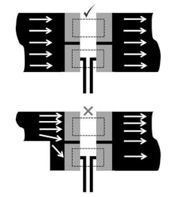
Moreover, this ensures that the proportion of the total current carried by the sensed resistor doesn’t vary with temperature. This would otherwise be the case with unequal series track resistances due to the high TCR of the copper PCB tracks.
Design for Heatsinking
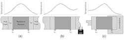
A flat-chip resistor dissipates more than 80% of its heat by conduction into PCB tracks, making it important to provide sufficient copper area to act as a heatsink. Copper area is, for this purpose, defined as the total area directly surrounding the solder pads, including the first two squares of connected tracks. Figure 9 indicates the general relationship between effective power rating and PCB copper area.
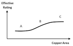
In region (A), there’s relatively low thermal conduction through copper connected to the pads, and conduction by substrate and convection to air predominate. In region (B), the copper connected to the pads acts as a heatsink to raise the effective power rating. In region (C), further increase in copper area gives diminishing returns, as the internal thermal impedance of the chip restricts the rating.
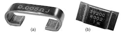
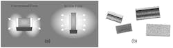
This limiting factor of the internal thermal impedance can be lowered significantly by changing the resistor’s orientation. If the terminations are formed on the longer edges of the chip rather than the shorter edges, the solder joint width is approximately doubled and the maximum distance from film center to termination is approximately halved (Fig. 10a). TT Electronics' ULR2N and ULR3N (Fig. 10b) are examples of products that use this enhanced cooling method.
The resistor datasheet should contain information on the mounting conditions used to obtain the rated power. This indicates the minimum copper area that should be provided by the designer.
Summary
The growing use of sub-milliohm chip resistors for current sensing creates a spectrum of challenges for the designer and the process engineer. The component format should first be selected to support the chosen thermal-management approach, with metal-element flat-chip resistors having two terminals being the most cost-effective solution. It’s then essential to design the PCB tracks and pads to meet the needs of the Kelvin connection, heat dissipation, and avoidance of induced noise.
Part 2 of this series will address additional stages, including verification of the ohmic value of unmounted components and critical assembly processes.
References
1. O’Sullivan, Marcus. “Optimize High-Current Sensing Accuracy by Improving Pad Layout of Low-Value Shunt Resistors,” Analog Dialogue 46-06 Back Burner, June 2012.
2. Folmar, Patrick. “The Truth about Placement Accuracy,” SST Semiconductor Digest.
Read the rest of the Overcome the Challenges of Using Sub-Milliohm SMD Chip Resistors series.
About the Author
Stephen Oxley
Business Development Engineer, Fixed and Variable Resistors, Sensors and Specialist Components division, TT Electronics
Stephen Oxley is Business Development Engineer for the Fixed and Variable Resistors, Sensors and Specialist Components division at TT Electronics . He has a master’s degree in electrical and electronic engineering from Bath University, the U.K.
Comment About the Article
To join the conversation, and become an exclusive member of Electronic Design, create an account today!

Leaders relevant to this article: