Three Major Design Pitfalls Plaguing New Analog Signal-Path Designers
This article is part of the TechXchange: Exploring Op Amps.
Members can download this article in PDF format.
What you’ll learn:
- How to interpret and extract clipping issues in signal-path components.
- Nuances in assessing output dc error bands.
- A quick and easy way to simulate phase margin.
Having been on the receiving end of designer queries from 1985 forward, there are some common oversights and misunderstandings that show up regularly. These essentially fall into three areas:
- Not considering the actual operating voltage range on the I/O or internal pins of the device being used.
- Misunderstanding the elements that contribute to an output dc offset or drift error.
- Accidentally building an oscillator (or even worse, a nominally stable design that slips over into oscillation over production and/or temperature ranges).
1. Running Into I/O Range Limits with Op Amps, FDAs, and INAs
The evolution of op amps began with very simple designs requiring considerable headroom to the supply voltages in both the input pins and the output pin. This carried over into the early fully differential amplifier (FDA) and instrumentation amplifier (INA) developments.
Over time, the need to provide more of the available supply voltage range on the I/O pins first led to rail-to-rail output (RRO) designs, then added negative rail input (NRI) designs, and more recently rail-to-rail input/output (RRIO) designs. These each come with compromises in the internals to the device.
Many single-supply designs will select at least a RRO and NRI device and then expect the device to operate with no input signal with the V+ and output pins at 0 V. All RRO devices require some small headroom to the supplies to operate linearly.
While that may be as low as 10 mV, it’s still not zero. Asking the op amp to perform as expected with 0-V input will usually cause performance problems. Most NRI devices can actually operate slightly below the negative supply; therefore, a 0-V input on a single-supply design usually will not hit an “input” limit.
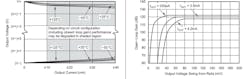
Another source of confusion has been the long-term evolution of how this “headroom” is specified. Early devices (still available) talk about a ground centered maximum ±VOUT swing on a bipolar supply. While accurate, it’s much more useful to think in terms of required headroom at the output (and input) to each supply voltage being used. Most early devices specified no load or a specified load for this swing.
The required headroom always increases as the demand escalates for more output current. This, and the open-loop gain reduction near the supplies, are captured in more recent op amps as shown in the curves of Figure 1 from the OPA350 datasheet (OPAx350 datasheet). While a true swing to ground is required in a single-supply design, some designs apply a fixed −0.23-V bias generator like the LM7705 (LM7705 datasheet).
The first commercial FDA—the AD8138—emerged in 1999. Subsequent developments have pushed towards extreme dc precision (and speed with low power) in mainly NRI and RRO designs like the THS4551 (THS4551 datasheet).
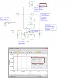
One common confusion when applying these modern FDAs is that a single-supply design can, in fact, take a dc-coupled bipolar input and operate all I/O pins with enough headroom on a single supply. The key here is that the common-mode (CM) control loop will force a dc level-shifting current back through the input resistors to level-shift the input CM voltage across the two inputs to operate above ground, even with a bipolar input signal. This effect is illustrated in Figure 2.
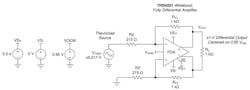
Any FDA circuit can reduce the input networks to Thevenin equivalents as shown in Figure 2. A good design will have equal feedback resistors and equal Thevenin impedances looking back from the two inputs to a source and ground (or low-impedance reference voltage).
The easiest way to see that the input CM voltages are above ground is to consider the lower output side of the FDA in Figure 2 dividing back to ground. If the output is correctly swinging ±0.5 V on each side around the stated 0.95-V CM voltage, the 0.45- to 1.45-V absolute swing on that lower output will divide back to the lower input pin as 0.177 × 0.45 V to 0.177 × 1.45 V equal to 80 to 256 mV.
Yes, the input CM voltage moves with the full-scale swing of the input signal but never goes below ground. Actually, since the outputs can’t go below ground, that feedback signal to the lower summing junction can’t swing below ground. The FDA differential loop forces the error voltage across the inputs to zero. Thus, the input pins move together for a single-ended input to differential output application.
A very popular solution in precision industrial applications is the instrumentation amplifier (INA). These typically present two high-impedance inputs with a settable differential gain to a single-ended output stage. Such an output often includes a reference voltage input that independently sets an output dc level separate from the input-signal-induced output swing.
Those all have specified input and output headrooms much like an op amp or FDA device. They also often have internal swing limits not directly observable in application or simulation. These hidden limits have tripped up many a design engineer.
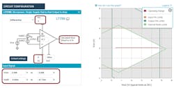
Several INA suppliers have developed tools to expose these limits in application. One is the instrumentation amplifier diamond plot tool (ADI Diamond Plot Tool for INAs). This tool allows designers to enter their intended input conditions and a desired gain and reference voltage, along with a candidate device, and immediately expose internal and external clipping issues.
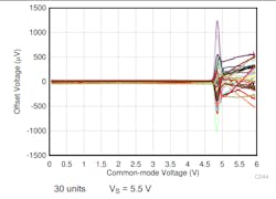
Figure 3 shows an example drawn from an actual thermocouple design where the input CM voltage is fixed at 2.048 using a single 5-V supply on the LT1789 INA. If the red line in the diamond plot is completely within the white area, unclipped operation is assured.
2. Designer Oversights in Assessing Output DC Precision and Drift
The calculations for output dc error and drift are well-trodden trails in academic and vendor material. Several detail issues continue to trip up new (as well as experienced) designers with the vast proliferation of op-amp and FDA solutions.
Classic bipolar input op amps and FDAs usually offer a well-matched input bias current error if it’s a voltage feedback amplifier (VFA). It’s effect on an output dc error can be reduced using a “bias current cancellation” resistor solution to reduce the output dc error to the offset current at the inputs (mismatch specification) times the feedback resistor value. For voltage-feedback op amps, this simply requires you to match the dc impedance looking out the V+ pin to the parallel combination of the feedback and gain resistors on the inverting side.
But where does this actually work—and not work? It will always work with simple NPN or PNP input stages having matched bias currents. Some very-low-bias-current bipolar input devices use cancellation currents into the input pins. If so, the offset currents aren’t as low as for the simpler input-stage designs. Bias currents are never matched for CMOS or JFET input devices, so designing for bias-current cancellation is a waste of time; lower R’s on the V+ pin are usually desirable to reduce added noise from those resistors.
Some of the very lowest input offset voltage and drift VFAs emerged with the chopper-input types of devices. These chopper-, and trimmed non-chopper-input, CMOS devices provide sub-10-μV input offsets with very low drift. Later developments added rail-to-rail input (RRI) options using crossover networks at the input to pass control between the CMOS device types. Zero-crossover RRI types include an on-chip boost regulator to provide enough supply voltage for the input stage to get RRI without a crossover network, like the OPA328 (OPA328 datasheet).
Those types of RRI devices with a crossover region will show a discontinuity in the input offset voltage as control is passed across the CM input range of the op amp. Many designers have been tripped up by this, where simply avoiding that area of the input CM might have been possible.
Figure 4 shows a good example from the recent OPA396 RRIO CMOS precision op amp (OPA396 datasheet), a non-chopper device quoting a maximum input offset of 100 μV. This gain-of-1 plot clearly shows the large step in input offset voltage near the positive supply. This is easily avoided by operating with a small non-inverting gain or running inverting mode with fixed bias on the V+ pin well below this crossover.
The very best input-drift VFA op amps use a chopper-input structure. Those intrinsically need an internal switching clock that then shows up in the input current noise spectrum. Though this often isn’t shown, it’s usually there. Whether this affects the accuracy in the application depends on many things, but at minimum it’s prudent to plan on at least a post-RC filter well below that chopping frequency to filter that off.
It’s also prudent for chopper-input op amps to design for source matching as in dc bias-current cancellation. This will reduce the higher-frequency output noise due to the chopper-input current spikes (“Reducing Chopper Input Artifacts” article). Some, but not all, chopper-input op amps report that chopping frequency.
CMRR and PSRR
The earliest op-amp literature spent quite some time discussing the common-mode rejection ratio (CMRR) and power-supply rejection ratio (PSRR) effects on output error terms. Those usually end up showing a plot over frequency that’s almost always a designer simulation as the measurement is nearly impossible.
Here, only the dc values are of interest for output dc error concerns. The PSRR gets confused in the datasheets, sometimes showing the supplies moving together—but that’s the same thing as a CMRR test. ATE flows move only one supply at a time to extract out an apparent shift in the input Vos voltage. These are often assumed to have a bipolar distribution in adding to the other dc error terms to get full output dc error band.
For typical single-supply designs with say a ±10% supply tolerance for a +5-V design, such an error term for modern devices is very small. Typical PSRR numbers are 110 dB or greater, so ±0.5-V supply shift in production maps to a ±1.6-μV expansion in the input offset span using a 110-dB specification.
CMRR has been presented as a shift in the input offset voltage as the CM input voltage travels across the available input span. In fact, all models and ATE data show this as a gain error term. Since the error is dependent on the input CM level, why would it be a static dc error when in fact it’s more like the LG/(LG+1) gain error (where LG is the loop gain, the Aol/(noise gain)). Often, this CMRR gain error is on same order or smaller than the Aol at a gain of 1, and it becomes even less significant at higher noise gains as that LG term becomes the dominant gain error.
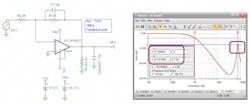
A simple simulation (Fig. 5) can easily illustrate what the model is producing. Here, the precision OPA837 (OPA837 datasheet) is set up with four equal resistors in a classic CMRR test. The output should be very close to zero swing, but here the input offset voltage is probed showing a very small 0.62-μV p-p amplitude square wave (around the nominal 40.6-μV offset voltage in the model) for a 1-V p-p CM input swing at the V+ input pin. Here a dependent unity-gain voltage buffer was inserted to isolate the V+ pin input resistance from the four-equal-resistor test setup.
The polarity indicates this model is showing a very small expansion in the gain due to CMRR effects. This 124-dB CMRR level will in practice combine with any gain error introduced by the LG/(LG+1) term. It’s not clear that this expanding gain effect in the OPA837 model is matching the physical device.
Both expanding and contracting CMRR effects can be found using different op-amp models in the test circuit of Figure 5. Holding a fixed (non-zero) input CM voltage (as in an inverting op-amp design) will add a fixed CMRR error contribution to the total input Vos calculation.
3. Ignore Nominal Design Phase Margin at Your Peril
Once we have the I/O ranges satisfied and the output dc error band estimated for particular candidate solution device, the actual functional design can proceed. Many different implementations and applications can call upon the vast range of op amps and FDAs for numerous end applications.
With a schematic and maybe even a layout developed, do you know your phase margin? Perhaps you should. Op amps have always had the risk of instability. It’s been exacerbated by the more aggressive designs in recent years trying to deliver the most performance at the lowest power.
For instance, the common RRO stage designs come with a very reactive open-loop output impedance (Fig. 6, “Improved Stability Analysis”). Hopefully this is in the simulation model. Often, it’s a little uncertain if this critical feature to loop phase margin is correctly captured by the model.
A circuit that’s already oscillating has one set of bench tools to isolate down to the suspect device. It’s for more prudent to attempt a phase-margin simulation prior to board build to head off any problems. That does, of course, depend on good simulation models, and those have been improving. Still, they come with a variety of pitfalls across the industry.
There are several easy techniques to extract the loop phase margin from an amplifier schematic (“Improved Stability Analysis”). If possible, any layout and source impedance parasitics should be added to the simulation, and by all means the intended load has to be there—even if it’s only a parasitic RC of the next device. Essentially, the simple techniques break the loop in some way, inject a small signal test signal in the loop, and trace the gain and phase around the loop to assess phase margin where the loop gain magnitude goes to 0 dB (or 1 V/V).
If we think about the transfer function having that LG/(LG+1) term, it can be rewritten as 1/(1+(1/LG)). The LG has a gain and a phase-shift component. If it drops close to a 1 magnitude (0 dB crossover) near where the phase shift is approaching 180 degrees around the loop, it becomes a 1/(1-1) term, which may result in sustained or intermittent oscillation. This can cost lots of manhours and re-spin dollars when a little bit of simulation time could have headed off this pain and suffering.
Even simple circuits can run into phase-margin problems (Fig. 6, again). Here, a simple inverting gain of −1-V/V design added a feedback capacitor to bandlimit the signal channel to 1 MHz. A small parasitic capacitive load, along with that feedback Cf, interacts with the reactive open-loop output impedance to cause the peaking at 74 MHz. This is a warning that the circuit might go unstable in production.
To run a LG phase-margin simulation, it’s necessary to first establish a good dc operating point for all nodes in the circuit. Older approaches found the exact input offset voltage to add to an open-loop circuit to zero the output-pin voltage. That works, but it’s much easier to use simulation tricks of impossibly high L and C elements to do this job for us, as shown in Figure 7 using the OPA837 model again.
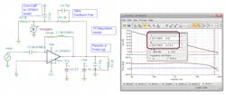
The large feedback inductor closes the feedback loop at dc, then immediately opens up on the first frequency test step. The large input capacitor is open at dc, then immediately shorts out to apply the test signal on the first frequency step.
This approach requires you to manually add the op-amp input impedance at the loop gain measurement point (2 pF here). The measurement meter is rotated to report phase margin directly for this setup. Looking for the 0-dB gain point around the loop and then the phase margin at that same 66.61-MHz frequency shows only 19.5 degrees. This would require some attention where several approaches (and this phase-margin simulation approach) are detailed in the OPA396 datasheet.
What your minimum target phase margin might be depends on your circuit and the device you’re using. Many older devices (National Semiconductor in particular) targeted a nominal 45 degrees and just took the peaking that results from it. More modern devices feature a nominal phase-margin target around 60 degrees to get close to a Butterworth closed-loop response. As a rough guideline for most circuits:
How sensitive a design is part to part and over temperature variation really depends on the circuit and devices chosen. Older op amps and FDAs have a wider spread on their open-loop gain and phase where more modern devices (especially those with supply current trim) are much better and will have far lower risk of large dips in phase margin over production.
Keep these three hazardous areas in mind as you set out to apply the vast range of op amps, FDAs, and INAs to your design.
Read more articles in the TechXchange: Exploring Op Amps.
About the Author

Michael Steffes
Analog Signal Path Consultant
Starting as an IC design engineer at the original current feedback amplifier company (Comlinear), I progressed through 35 years of high speed amplifier development projects. Through these years I contributed to the definition, development, and product launch (datasheets and simulation models) of over 150 high speed amplifiers. Generating the related technical collateral also produced over 150 contributed articles and application notes..
Comment About the Article
To join the conversation, and become an exclusive member of Electronic Design, create an account today!

Leaders relevant to this article: