Basic Guidelines for Mixed-Signal PCB Layout Design
This article is part of the TechXchange: PCB Tools and Technology.
Members can download this article in PDF format.
What you'll learn:
- Considerations for dividing analog and digital blocks.
- Decoupling techniques.
- Breaking down the board layers.
- How best to deal with grounding.
A mixed-signal printed-circuit-board (PCB) design requires basic understanding of analog and digital circuitry to minimize, if not prevent, signal interference. Modern systems consist of components that are operational with both digital and analog domains, and they must be carefully designed to ensure signal integrity all throughout the system.
PCB layout—an important part of the mixed-signal development process—can be intimidating and component placement is just the beginning. Other factors must be considered, too, including board layers and how to properly manage them to minimize interference caused by parasitic capacitors that can be unintentionally created between the PCB’s interplane layers.
Grounding also is an integral process in the PCB layout design of a mixed-signal system. While grounding is a frequently debated topic in the industry, constructing a standardized approach may not always be the simplest task for any engineer. For instance, a single issue of quality grounding can affect the entire layout of a high-performance mixed-signal PCB design. And for this reason, this area should not be overlooked.
Component Placement
Similar to building a house, it’s essential to create a floorplan of the system before placing the circuit components. This step will set the overall integrity of the system design and should help avoid noisy signal interference.
In developing a floorplan, it’s advisable to follow the signal path of the schematic, especially for high-speed circuits. The location of a component also is a critical aspect of the design. The designer should be able to identify the important functional blocks, signals, and the connection between the blocks to identify the best fit location of each component in the system. Connectors, for instance, are better placed on the edges of the board, while auxiliary components such as decoupling capacitors and crystals must be placed as close as possible to the mixed-signal device.
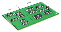
Analog and Digital Blocks Partition
To help minimize the common return path for analog and digital signals, analog and digital block separation may be considered so that analog signals will not mix with digital signals.
Figure 1 shows a good example of analog and digital circuit separation. Some considerations when separating analog and digital sections include:
- Sensitive analog components such as amplifiers and voltage references are recommended to be placed within the analog plane. Similarly, noisy digital components like logic controls and timing blocks must be placed on the other side/digital plane.
- If a system contains one mixed-signal analog-to-digital converter (ADC) or a digital-to-analog converter (DAC) with low digital currents, this can be treated similar to analog components in the analog plane.
- For designs with more than one ADC and DAC with high current, it’s recommended to split the analog and digital supplies. That is, AVCC must be tied to the analog section while DVDD should be connected to the digital section.
- Microprocessors and microcontrollers may take up space and will generate heat. These components must be placed in the center of the board for better thermal dissipation, and, at the same time, close to their related circuit blocks.
Power-Supply Block
The power supply is an important part of the circuit and should be handled accordingly. As a rule of thumb, the power-supply block must be isolated from the rest of the circuitry while remaining close to the components being powered.
Complex systems with devices that have multiple supply pins can use separate power-supply blocks dedicated for the analog and digital sections to avoid noisy digital interference.
On the other hand, power-supply routing should be short, direct, and use wide traces to reduce inductance and avoid current limitation.
Decoupling Techniques
Power-supply rejection ratio (PSRR) is an important parameter a designer must consider when trying to achieve target system performance. PSRR is the measure of the sensitivity of a device with respect to power-supply variations, which will eventually dictate the performance of a given device.
To maintain an optimum PSRR, it’s necessary to keep the high frequency energy from entering the device. This can be done by properly decoupling the device’s power supply to the low-impedance ground plane with a combination of electrolytic and ceramic capacitors.
The whole concept of correct decoupling is to develop a low-noise environment in which the circuit can operate. The basic rule is to make it easy for the current to return by providing the shortest path.
Designers must always check the high-frequency filtering recommendation of each device. More so, this checklist will serve as a guide by providing general decoupling techniques and their correct implementation:
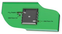
- While electrolytic capacitors act as charge reservoirs to transient currents to minimize low-frequency noise on power supplies, low-inductance ceramic capacitors reduce high-frequency noise. Also, ferrite beads are optional but will add extra-high-frequency noise isolation and decoupling.
- Decoupling capacitors must be placed as close as possible to the power-supply pins of the device. These capacitors should connect to a large area of low-impedance ground plane through a via or short trace to minimize additional series inductance.
- The smaller capacitor, typically 0.01 to 0.1 μF, should be placed as close as physically possible to the power pins of the device. When the device has several outputs switching at the same time, this placement prevents instabilities. The electrolytic capacitor, typically 10 to 100 μF, should be placed no more than one inch away from the power pin of the device.
- For easier implementation, decoupling capacitors can be linked through a T-type connection to the ground plane using vias near the GND pin of the component rather than creating a trace. See the sample in Figure 2.
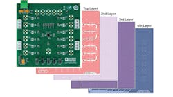
Board Layers
Once component placement and the floorplan have been set, we can go through the other dimension of the board design, commonly referred to as board layers. It’s highly recommended that board layers be considered first before doing the PCB routing, as this will determine the allowable return current paths of the system design.
A board layer is the vertical arrangement of the copper layers in the board. These layers should manage the currents and signal throughout the board.
A visual representation of the board layers is shown in Figure 3. The table details a typical four-layer PCB setup.
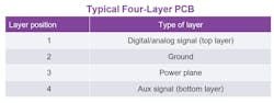
In general, high-performance data-collecting systems should have four or more layers. The top layer is often used for digital/analog signals, while the bottom layer handles auxiliary signals. The second layer (ground layer), which serves as a reference plane for impedance-controlled signals, reduces IR drops and shields the digital signals in the top layer. Finally, the power plane is on the third layer.
Power and ground planes must be adjacent to each other as they provide additional interplane capacitance, which helps with the high-frequency decoupling of the power supply.
For the ground layer, advice has changed over the years for the mixed-signal design. Over the years, splitting the ground plane between analog and digital has made sense, but for modern mixed-signal devices, a new approach is recommended. Proper floorplanning and separating signals should prevent any issues with noisy signals.
Ground Plane: To Split or Not to Split?
Grounding is an essential process in the layout design of a mixed-signal PCB. A typical four-layer PCB must have at least one layer dedicated to the ground plane to ensure a low-impedance path for return signals. All integrated-circuit ground pins should be routed and connected correctly to the low-impedance ground plane to minimize the series inductance and resistance.
It’s become a standard grounding approach for mixed-signal systems to separate analog and digital ground. However, mixed-signal devices with low digital current can be best managed with a single ground. Moving forward, a designer must consider which one of two grounding practices suits best, depending on the mixed-signal current requirement.
Single Ground Plane
For mixed-signal systems with a single ADC or DAC that has low digital current, a solid single ground plane would be the best approach. To understand the importance of a single ground layer, we need to recall return current. Return current is the current that flows while returning to ground and traces between devices to complete a loop. To prevent mixed-signal interference, each return path must be tracked throughout the PCB layout.
The simple circuit in Figure 4 shows the advantage of a single solid ground plane over a split ground plane. The signal current has an equal but opposite flow of return current. This return current flows in the ground plane back to the source, following the path of least impedance.
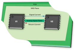
For low-frequency signals, the return current will take the path of least resistance, usually a straight line between the ground reference points of the devices. However, for higher-frequency signals, a certain portion of the return current will try to follow the signal path back. That’s because the impedance is lower following this path, since it minimizes the size of the loop formed between the outgoing and returning current.
Analog and Digital Ground Separation
For complex systems in which a solid ground scheme can be challenging to achieve, a split ground may be more appropriate. A split ground plane is popular approach where the ground plane is split in two: analog and digital ground planes. This is applicable for more complex systems with multiple mixed-signal devices consuming high digital current. Figure 5 shows a system with a split ground plane.
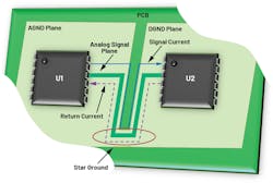
For systems with a split ground plane, the simplest way to achieve a cohesive ground is to remove the break in the ground planes and enable the return current to take a more direct route through a star ground junction. The star ground is the junction where the analog and digital ground planes are joined together on a mixed-signal layout design.
In common systems, the star ground can be associated with a simple narrow continued junction in between analog and digital ground planes. For more complex designs, the star ground is commonly implemented with a jumper shunt to a ground header. No high current carrying a header and jumper shunt is required because there will be no flow of current in the star ground. Rather, its main purpose is to make sure that both grounds have the same reference levels.
Designers must always check grounding recommendations found in each device’s datasheet to ensure grounding specifications will be met and avoid ground-related issues.
On another note, for mixed-signal devices with AGND and DGND pins, these can be tied to their respective ground planes since the star ground also will connect both grounds at one point. In this way, all noisy digital currents will flow through the digital power supply down to the digital ground plane and back to the digital supply while being isolated from the sensitive analog circuitry. Isolation of the AGND and DGND planes must be implemented on all layers of a multilayer PCB.
Other Common Grounding Practices
This procedure/checklist can help to ensure an appropriate grounding scheme has been implemented in a mixed-signal analog/digital system:
- Wide copper traces should make up the connections at the star point.
- Check the ground plane for narrow traces, as these connections are undesired.
- It’s useful to provide pads and vias so that the analog and digital ground planes can be connected, if necessary.
Conclusion
The PCB layout for mixed-signal applications can be challenging. Creating a component floorplan is just the starting point. Properly managing board layers and preparing an adequate grounding scheme also are part of the key points a system designer must consider when trying to achieve optimum performance in a mixed-signal system layout.
Preparing a component floorplan will help set the overall integrity of the system design. Proper board-layer organization will help manage the currents and signal throughout the board. Finally, choosing the most beneficial grounding scheme will improve the system’s performance and prevent any issues with noisy signals and return current.
Acknowledgement
The material presented in this article was compiled from many contributors, including Eric Carty, Genesis Garcia, Giovanni Aguirri, Brendan Somers, Stuart Servis, Leandro Peje, Mar Christian Lacida, and Yoworex Tiu.
Read more articles in the TechXchange: PCB Tools and Technology.
References
Walt Kester, The Data Conversion Handbook. Analog Devices, Inc., 2005.
John Ardizzoni, “A Practical Guide to High-Speed Printed-Circuit-Board Layout.” Analog Dialogue, Vol. 39, No. 9,
September 2005.
Ralph Morrison, Grounding and Shielding Techniques. John Wiley & Sons, Inc., 1998.
Thomas O’Shea, “AN-1349 Application Note: PCB Implementation Guidelines to Minimize Radiated Emissions on the ADM2582E/ADM2587E RS-485/RS-422 Transceivers.” Analog Devices, Inc., August 2018.
“MT-101 Tutorial Decoupling Techniques.” Analog Devices, Inc., 2009.
Linear Circuit Design Handbook. Analog Devices, Inc., 2008.
Paul Brokaw, “AN-342 Application Note, Analog Signal-Handling for High Speed and Accuracy.” Analog Devices, Inc.
Walt Kester, James Bryant, and Mike Byrne, “MT-031 Tutorial Grounding Data Converters and Solving the Mystery of ‘AGND’ and ‘DGND’.” Analog Devices, Inc., 2009.
Paul Brokaw and Jeff Barrow, “AN-345 Application Note: Grounding for Low- and High-Frequency Circuits, Know Your Ground and Signal Paths for Effective Designs, Current Flow Seeks Path of Least Impedance–Not Just Resistance.” Analog Devices, Inc.
Doug Grant and Scott Wurce, “AN-348 Application Note: Avoiding Passive Component Pitfalls, The Wrong Passive Component Can Derail Even the Best Op Amp or Data Converter Here Are Some Basic Traps to Watch For.” Analog Devices, Inc.
About the Author
May Anne Porley
Applications Engineer, Analog Devices Inc.
May Anne Porley is an applications engineer at Analog Devices in the Philippines, within the Automated Test Equipment (ATE) Group. She joined ADI in 2012 and provides applications support for switches, multiplexers, level translators, and unbuffered crosspoint switches portfolios. May Anne graduated from De La Salle University—Dasmariñas, Philippines, with a bachelor’s degree in electronics engineering.
Comment About the Article
To join the conversation, and become an exclusive member of Electronic Design, create an account today!

Leaders relevant to this article: