CMOS Acoustic MEMS Structure Yields On-Chip 8- to 12-GHz Resonator
What you’ll learn:
- How standard CMOS process can be used for an on-chip gigahertz resonator.
- How multiple modeling tools were used to design the device and understand the impact of design variations.
- How the resultant design yielded a high-Q on-chip resonator operating above 10 GHz.
High-frequency resonators are key elements in both filters and voltage-controlled oscillators. Recent developments in this area include thin-film bulk acoustic resonators with ferroelectric materials, as well as high-frequency Lamb- and Lamé-wave resonators using piezoelectric lithium-niobate or aluminum-nitride thin films. The demands of 5G designs are placing even more emphasis on higher levels of on-chip integration to reduce both component count and system size.
Now, a team at Purdue University has pursued the use of phononic-crystal (PnC) confinement that could enable resonator integration directly into a standard CMOS process, thus potentially leading to larger multiple-input/multiple-output (MIMO) arrays in a smaller footprint at lower power.
The devices use phononic waveguides for acoustic confinement and exploit MOS capacitors and transistors to electromechanically drive and sense acoustic vibrations. Their CMOS fin field-effect transistor (FinFET)-based resonators employ acoustic waveguiding confinement operating in the X-band of 8 to 12 GHz.
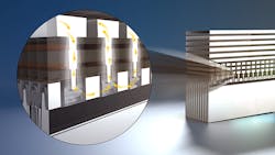
Their resonator structure, referred to as a fin-resonant body transistor (fRBT) (Fig. 1), uses a standard commercial GlobalFoundries process and required just 9 × 15 μm. The four-port network is differentially driven between adjacent gates along the fin length with the resonator’s output taken as the differential transconductance.
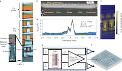
1. Overview of FinFET resonator: (a) Cross-section of one period of the FinFET resonator, modeled in COMSOL, with the inset highlighting the Si fin (dark green) and epitaxial raised source and drain with silicide. The metal and contact layers are highlighted in orange and dark grey, respectively, and the dielectric layers are colored blue and green. (b) Representative acoustic cavity, consisting of a sense block sandwiched between two drive blocks, with terminations at either end to increase acoustic confinement. (c) Mode displacement. (d) Experimentally measured mode, with f0Q product of 8.2 × 10¹¹, placing it within an order of magnitude of the released MEMS resonators. (e) Combined with a differential transconductance amplifier, the fRBT enables a high-frequency mechanically referenced two-phase oscillator in the standard CMOS process. (f) Acoustically coupled (blue lines) network of oscillators in CMOS FEOL with local electrical clock routing (bronze lines), eliminating power-hungry phase-locked loops used for clock distribution.
This transconductance is primarily a function of three main factors: the electrical-to-acoustic transduction efficiency in the drive transistors, acoustic-energy confinement and amplification in the resonance cavity, and acoustic-to-drain current conversion in the output transistors.
The initial device design focused on maximizing the acoustic energy confinement by varying the gate length, termination scheme, and back-end-of-line (BEOL) confinement conditions. By integrating a PnC at the BEOL of the standard CMOS process and leveraging the mechanical bandgaps of such structures, they were able to effectively confine the energy and thus boost the resonance Q factor (Fig. 2).
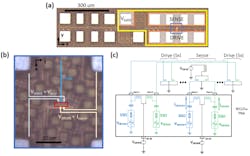
2. (a) Die micrograph showing two adjacent resonators, with ground/signal (GSS) pads for the RF drive and sense and a DC pad for gate biasing. b) Close-up view from center of device in (a), showing the approximate resonator location, dimensions, and signal routing underneath the BEOL metal layers. (c) Device measurement setup, with differential RF input applied via ports one and three of a Keysight N5225a Performance Network Analyzer (PNA). Differential output current measured via ports two and four; dc gate bias is applied directly from a Keithley 2400 Source Measure Unit (SMU) using a needle probe, while the drive and drain biases are applied via SMU through the PNA using the built-in bias-tee.
To study and optimize the bandgap induced by the PnCs, multiple 3D simulations were performed in COMSOL Multiphysics. To understand the conversion from stress to drain current in the sense transistors, they modeled the modulation of three separate FET properties: oxide capacitance, channel mobility due to piezoresistivity, and silicon bandgap (Fig. 3).
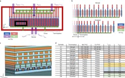
3. Variations in resonant-cavity design: (a) Top-down view of the device shows the central sense transistors with five pairs of capacitors on either side, allowing for a differential drive, capped on either end by termination (10 gates in the actual devices, abbreviated to three in the figure) and surrounded by a ground ring. The first-level metal M1 is used for routing within the structure, whereas higher-level metals in Mx and Cx (not shown for clarity in this diagram) rest above this routing in either the continuous plate or the PnC form. (The Kx layer represents higher-level metal layers used for device-to-pad routing.) (b) Depiction of termination schemes investigated for use at the ends of the resonant cavity. (c) View of a subset of the resonant cavity of devices A3 and A4, showing fins extending in the x direction and gates extending into the y direction. (d) Variations in device design that were implemented and tested.
This model has only a handful of parameters to describe the device’s operation. Typically, the more advanced BSIM model commonly used in industry includes many empirically fit parameters to give the best device models for commercial applications. They used other modeling and data-analysis techniques, including analysis of variance (ANOVA), to quantify the impact of the many variations in device design on the spectrum of acoustic modes.
Their results demonstrated how the acoustic perturbation of carrier effective mass simultaneously modulates the saturation velocity and mobility. PnC confinement was experimentally shown to be the most important parameter in improving the unreleased resonator performance with an improvement on average of ≈2.2. It also provides a significant opportunity for integrating acoustic devices into standard CMOS platforms.
Their highest-performing resonator—a gradually terminated device with 80-nm gate-length—exhibited a transconductance amplitude of 4.49 μs and Q of 69.8 in the 11.73-GHz mode, corresponding to an f × Q product of 8.2 × 10¹¹. The Purdue team concluded that this technology could be used to develop compact, low-cost, CMOS-integrated and electrically controllable resonators that require no additional packaging.
The work is detailed in their nine-page paper “Integrated acoustic resonators in commercial fin field-effect transistor technology” (pdf version here) published in Nature Electronics. It’s supported by a more-detailed 19-page Supplementary Information file that provides deep-physics and modeling equations, code segments, and comprehensive results.
About the Author

Bill Schweber
Contributing Editor
Bill Schweber is an electronics engineer who has written three textbooks on electronic communications systems, as well as hundreds of technical articles, opinion columns, and product features. In past roles, he worked as a technical website manager for multiple topic-specific sites for EE Times, as well as both the Executive Editor and Analog Editor at EDN.
At Analog Devices Inc., Bill was in marketing communications (public relations). As a result, he has been on both sides of the technical PR function, presenting company products, stories, and messages to the media and also as the recipient of these.
Prior to the MarCom role at Analog, Bill was associate editor of their respected technical journal and worked in their product marketing and applications engineering groups. Before those roles, he was at Instron Corp., doing hands-on analog- and power-circuit design and systems integration for materials-testing machine controls.
Bill has an MSEE (Univ. of Mass) and BSEE (Columbia Univ.), is a Registered Professional Engineer, and holds an Advanced Class amateur radio license. He has also planned, written, and presented online courses on a variety of engineering topics, including MOSFET basics, ADC selection, and driving LEDs.
Comment About the Article
To join the conversation, and become an exclusive member of Electronic Design, create an account today!

Leaders relevant to this article: