Photonic IC Brings High-Performance Reconfigurable Filtering to Microwave Signals
This article appeared in Microwaves & RF and has been published here with permission.
What you’ll learn:
- How photonics can provide high-performance RF filtering.
- The photonics topology used to implement the principles.
- Results of various performance tests.
It may seem at first glance that the electronic circuit/RF world and the photonic-device worlds are two distinct and separate settings. But that’s not the case at all, and many photonics devices are finding roles in microwave RF applications.
Microwave photonics (MWP) is an interdisciplinary research field that develops technologies to generate, process, and distribute RF/microwave signals using optical components. While a number of integrated MWP functions, such as filter, phase shifter, delay line, and beamforming, have been developed, these circuits need to show advanced reconfigurability and high RF performance in terms of loss, noise figure, and dynamic range to be viable in real RF applications.
A research team at the University of Twente (Enschede, Netherlands) has developed a programmable, integrated MWP circuit with high integration density, versatile reconfigurability, and impressive RF performance. They created reconfigurable filter functions with record-low noise figure and a RF notch filter featuring ultra-high dynamic range.
The MT and DI-RR
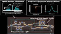
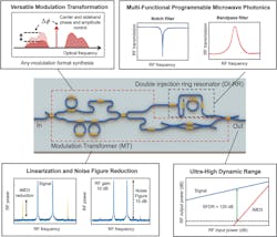
They did this using versatile, complex spectrum tailoring enabled by an all-integrated modulation transformer (MT) and a double-injection ring resonator (DI-RR) as a multifunction optical-filtering component (Fig. 1). The team also introduced two techniques for enhancing RF performance: optical carrier suppression and a low-biasing Mach Zehnder modulator.
The MT can independently tailor the phase and amplitude of any input optical modulation spectrum and convert the spectrum into different output optical modulations (Fig. 2). The DI-RR is able to synthesize six different responses from a single output; four different proof-of-concept scenarios were presented using the new circuit.
The circuit with combined MT and DI-RR synthesized MWP bandstop-bandpass reconfigurable filters with high RF performance. The MWP bandstop/notch filter had 58-dB rejection with 10 dB of RF gain and 15-dB noise figure (NF). With proper tuning, the filter could be reconfigured into an MWP bandpass filter with 20 dB of rejection, 1.2 dB of RF gain, and 21.8 dB NF.
These results showed that the new circuit has versatile filtering functions along with superior RF performance. However, despite these achievements, the filter bandwidths of the new circuit were still in the order of hundreds of MHz, which isn’t sufficient for some RF applications.
Boosting Bandwidth with SBS
To overcome this challenge and create an MWP filter with a narrow bandwidth, a nonlinear optical effect known as stimulated Brillouin scattering (SBS) was introduced to the system. SBS is a third-order nonlinear property in an optical medium that’s created from the interaction of optic and acoustic waves in a waveguide.
Thus, in the next circuit design, a spiral waveguide capable of induced SBS was added to the system. Together with MT and DI-RR, this new circuit aimed to create a programmable MWP Brillouin filter with a reconfigurable narrow bandwidth and high RF performance.
The waveguides were fabricated using a standard photonics IC process. First, a SiO2 layer was grown from wet thermal oxidation of single-crystal silicon substrate at temperatures above 1000°C. Low-pressure chemical-vapor deposition (LPCVD) was then used for the Si3N4 layers, together with the gas tetraethylorthosilicate (TEOS) for the intermediate SiO2 layer. Subsequently, the waveguides were patterned using contact lithography, and processed with dry etching. Finally, the waveguides were covered with an additional SiO2 layer through LPCVD TEOS.
Test Results
Performance of the core MT and DI-RR was assessed against wide range of relevant factors (Fig. 3).
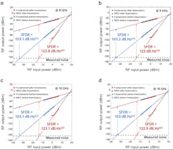
The end-to-end performance was also characterized with respect to many parameters, including (but not limited to) spurious-free dynamic range (SFDR) measurements at various two-tone frequencies with notch response at 12 GHz (Fig. 4).
Prof. Dr. David Marpaung, one of the authors of the study, summed it up this way: ”Solving the noise figure and dynamic range problem is one of the hardest challenges in microwave photonics. This breakthrough proves that integrated microwave photonics can indeed achieve very high performance.”
The work is detailed in their eight-page paper “Ultrahigh dynamic range and low noise figure programmable integrated microwave photonic filter” published in Nature Communications. It’s bolstered by a 16-page Supplementary Information file that has substantially more details on design, fabrication, equations, analysis, and test results.
About the Author

Bill Schweber
Contributing Editor
Bill Schweber is an electronics engineer who has written three textbooks on electronic communications systems, as well as hundreds of technical articles, opinion columns, and product features. In past roles, he worked as a technical website manager for multiple topic-specific sites for EE Times, as well as both the Executive Editor and Analog Editor at EDN.
At Analog Devices Inc., Bill was in marketing communications (public relations). As a result, he has been on both sides of the technical PR function, presenting company products, stories, and messages to the media and also as the recipient of these.
Prior to the MarCom role at Analog, Bill was associate editor of their respected technical journal and worked in their product marketing and applications engineering groups. Before those roles, he was at Instron Corp., doing hands-on analog- and power-circuit design and systems integration for materials-testing machine controls.
Bill has an MSEE (Univ. of Mass) and BSEE (Columbia Univ.), is a Registered Professional Engineer, and holds an Advanced Class amateur radio license. He has also planned, written, and presented online courses on a variety of engineering topics, including MOSFET basics, ADC selection, and driving LEDs.


![3. Programmable integrated MWP circuit: (a) The optical image of the programmable photonic chip with outlined waveguide leads, containing a modulation transformer (MT) and a double-injection ring resonator (DI-RR). The MT consists of a spectral de-interleaver used to isolate one RF sideband from the entire modulated spectrum. The phase shifter and tunable coupler are used to control the phase and amplitude of the isolated sideband. Modulation transformation is achieved after recombination at the output. (b) Experimental result of intensity-to-phase modulation (IMPM) conversion with 62-dB extinction, achieved using the MT with IM input. (c) Measured phase-to-intensity modulation (PMIM) conversion with 64-dB extinction, achieved using the MT with PM input. The DI-RR circuit is utilized to synthesize multiple filter functionalities. (d-g) Simulated (blue line) and measured (black line) selected responses of the silicon-nitride DI-RR when tuned to exhibit notch filter (d), bandpass filter (e), fano-like response (f), and all-pass response (g). [Note: “fano response” is a type of resonant-scattering phenomenon that results in an asymmetric line shape.] 3. Programmable integrated MWP circuit: (a) The optical image of the programmable photonic chip with outlined waveguide leads, containing a modulation transformer (MT) and a double-injection ring resonator (DI-RR). The MT consists of a spectral de-interleaver used to isolate one RF sideband from the entire modulated spectrum. The phase shifter and tunable coupler are used to control the phase and amplitude of the isolated sideband. Modulation transformation is achieved after recombination at the output. (b) Experimental result of intensity-to-phase modulation (IMPM) conversion with 62-dB extinction, achieved using the MT with IM input. (c) Measured phase-to-intensity modulation (PMIM) conversion with 64-dB extinction, achieved using the MT with PM input. The DI-RR circuit is utilized to synthesize multiple filter functionalities. (d-g) Simulated (blue line) and measured (black line) selected responses of the silicon-nitride DI-RR when tuned to exhibit notch filter (d), bandpass filter (e), fano-like response (f), and all-pass response (g). [Note: “fano response” is a type of resonant-scattering phenomenon that results in an asymmetric line shape.]](https://img.electronicdesign.com/files/base/ebm/electronicdesign/image/2023/05/ED_Photonic_microwave_filter_interest_Fig3.646691f94c09d.png?auto=format,compress&fit=max&q=45?w=250&width=250)
