Product Cascade Shows Vitality of Analog Building-Block Devices

With all of the attention given to highly integrated, high-functionality mixed-signal ICs targeting various application niches, it’s easy to presume that there’s no need for new basic, single-function analog ICs. It almost feels as if all we need is already available as seen in the vendors’ selection guides. For example, a myriad of basic op amps offer what seems to be every possible combination of attributes that anyone would demand (except the mythical “ideal” op amp).
Nonetheless, if you think it’s all over for new analog building blocks, you’d be wrong. Despite the broad and deep selection of available devices, there’s still a need for new, basic devices featuring improvements in one or more characteristics.
Proof of this is in these four single-function components recently introduced by Texas Instruments (and it’s not just TI; their competitors are doing similar). A look at these ICs—a programmable-gain amplifier (PGA), window comparator, RF-optimized voltage regulator, and automotive op amp—provides incontrovertible evidence of our apparent insatiable desire for more of these improved analog-function blocks.
The ICs serve in multiple roles: as the analog equivalent of what used to be called “glue logic” for interfacing disparate subfunctions, as front-end components that serve as transducer small-signal gateways, and even as critical auxiliary functions ensuring that other components can achieve their full performance potential:
1. PGA855: Low-noise, fully-differential-output PGA with high bandwidth across all gains
The PGA855 is a high-bandwidth programmable-gain instrumentation amplifier with fully differential outputs. It features eight binary-value gain settings spanning an attenuating gain of 0.125 V/V to a maximum gain of 16 V/V using three digital-gain selection pins (Fig. 1).
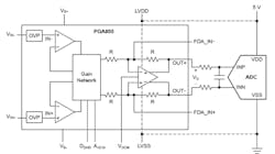
The architecture is optimized to drive inputs of high-resolution, precision analog-to-digital converters (ADCs) with sampling rates up to 1 Msample/s without the need for an additional ADC driver. The super-beta input transistors offer extremely low input-bias current, which in turn yields a very low input-current noise density of 0.3 pA/√Hz, making the PGA855 a good choice for almost any sensor type.
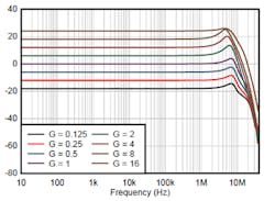
Furthermore, the low-noise current-feedback front-end architecture offers excellent gain flatness even at high frequencies (Fig. 2). Thus, the PGA855 becomes an excellent high-impedance sensor readout device.
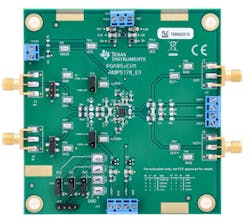
Housed in a 3- × 3-mm QFN, the IC is supported by a comprehensive 28-page datasheet as well as the PGA855 evaluation module (Fig. 3). The EVM, with a 21-page User’s Guide, provides access to features and measures performance. It includes subminiature version A (SMA) connectors and test points for quick tests, and offers access to output-voltage common-mode (VOCM) control and VO+ and VO- pins for detailed evaluation.
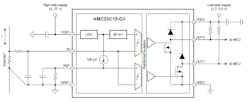
2. AMC23C15-Q1: Automotive, dual fast-response reinforced-isolated-window comparator with adjustable threshold
The AMC23C15-Q1, a dual isolated-window comparator with a fast response time, is optimized for overcurrent- or overvoltage-detection situations. The open-drain outputs are separated from the input circuitry by an isolation barrier that’s highly resistant to magnetic interference. This barrier is certified to provide reinforced galvanic isolation of up to 5 kVRMS , according to VDE 0884-17 and UL1577, and supports a peak working voltage of up to 1 kV (Fig. 4).
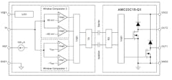
Both comparators have windows centered around 0 V, meaning that the comparators trip if the input exceeds the thresholds in a positive or negative direction. One comparator has fixed thresholds of ±60 mV. The second comparator has adjustable thresholds from ±5 to ±300 mV through a single external resistor. In a typical application, it’s used with a current-sensing shunt resistor (Fig. 5).
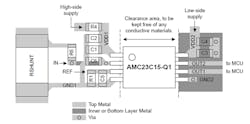
The AMC23C15-Q1, which is AEC-Q100-qualified for automotive applications, is housed in a wide-body 8-pin SOIC package and operates over the −40 to +125°C temperature range. Among other application insights, the 42-page datasheet includes a recommended layout that facilitates meeting regulatory mandates (Fig. 6).
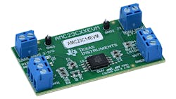
There’s also the AMC23C14EVM evaluation module that facilitates assessment of the device, and which is supported by a 10-page User’s Guide (Fig. 7).
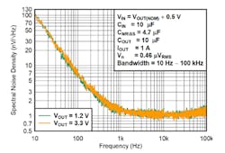
3. TPS7A96: 2-A, ultra-low-noise, ultra-high-PSRR RF voltage regulator
The TPS7A96 is an ultra-low noise (0.46 μVRMS), low-dropout (LDO) voltage regulator that can source up to 2 A with only 200 mV of dropout (Fig. 8). This LDO, in conjunction with a wide-bandwidth error amplifier, allows for very high power-supply rejection ratio (PSRR) of 110 dB at 1 kHz and 50 dB at 1 MHz under low operating headroom (500 mV) and high output current (1.75 A).
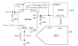
It’s designed to power sensitive analog low-voltage devices such as RF and imaging front ends, where any noise degrades signal-to-noise ratio and bit error rate and (Fig. 9). The device output is resistor-adjustable from 0 to 5.5 V via an external resistor. With the wide input-voltage range, the TPS7A96 supports operation as low as 1.9 V and up to 5.7 V. It includes a programmable current limit, programmable power-good threshold, and precision enable, all allowing for better control in the application.
The regulator features 1% output-voltage accuracy (over line, load, and temperature) and soft-start capabilities to reduce inrush current, Further, this LDO, in its 3.00- × 3.00-mm, 10-pin WSON package, can be easily paralleled for even lower noise and higher current.
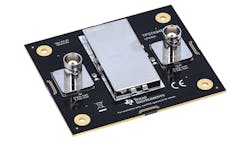
Despite its presumed functional simplicity, it’s accompanied by a 53-page datasheet and the TPS7A94 evaluation module (EVM) that helps design engineers evaluate the operation and performance of the linear regulator for use in their own circuit application (Fig. 10).
4. TLV9161-Q1: Automotive 16-V, 11-MHz rail-to-rail input/output operational amplifier
Finally, what can be more fundamental than an op amp? The TLV916x-Q1 family (TLV9161-Q1, TLV9162-Q1, and TLV9164-Q1) of 16-V, general-purpose, automotive-qualified op amps serves diverse, focused applications in this challenging electrical and thermal environment (Fig. 11).
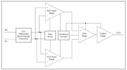
They offer exceptional dc precision and ac performance, including rail-to-rail input or output, low offset voltage (±210 µV, typical), low offset-voltage drift (±0.25 µV/°C, typical), low bias current (±10 pA), low noise (6.8 nV/√Hz at 1 kHz, 4.2 nV/√Hz at 10 kHz) and high common-mode rejection (110 dB), all of which simplify design-in and error budgeting.
Among other features are a wide differential-input voltage range, high short-circuit current (±73 mA), and high slew rate (33 V/µs), all of which contribute to its “multiplexer-friendly” front end.
Despite the functional simplicity of these components, the family is supported by a comprehensive 45-page datasheet that includes numerous performance tables and graphs, application information and relevant calculations, and suggested PCB layouts to optimize performance. The op amps come in a wide range of package sizes and pin counts to meet different user preferences.
About the Author

Bill Schweber
Contributing Editor
Bill Schweber is an electronics engineer who has written three textbooks on electronic communications systems, as well as hundreds of technical articles, opinion columns, and product features. In past roles, he worked as a technical website manager for multiple topic-specific sites for EE Times, as well as both the Executive Editor and Analog Editor at EDN.
At Analog Devices Inc., Bill was in marketing communications (public relations). As a result, he has been on both sides of the technical PR function, presenting company products, stories, and messages to the media and also as the recipient of these.
Prior to the MarCom role at Analog, Bill was associate editor of their respected technical journal and worked in their product marketing and applications engineering groups. Before those roles, he was at Instron Corp., doing hands-on analog- and power-circuit design and systems integration for materials-testing machine controls.
Bill has an MSEE (Univ. of Mass) and BSEE (Columbia Univ.), is a Registered Professional Engineer, and holds an Advanced Class amateur radio license. He has also planned, written, and presented online courses on a variety of engineering topics, including MOSFET basics, ADC selection, and driving LEDs.
Comment About the Article
To join the conversation, and become an exclusive member of Electronic Design, create an account today!

Leaders relevant to this article: