Graphene-Based Transistors Receive R&D and Mass-Media Attention
This article is part of the TechXchange: Distinguishing Discretes.
What you’ll learn:
- Why carbon-derived graphene is attracting research attention.
- How graphene is transformed into a potentially useful semiconductor device.
- Some of the challenges overcome in making this graphene transformation.
There’s something fascinating about elemental carbon. The atoms of carbon can bond together in diverse ways, yielding allotropes (different structural forms) such as graphite, diamond, amorphous carbon, and fullerenes.
Yet that’s only part of carbon’s story. Its physical properties vary widely with the allotropic form: graphite is opaque and black, while diamond is highly transparent. Graphite is soft enough to create streaks on paper while diamond is the hardest naturally occurring material known. Graphite is a good electrical conductor while diamond has low electrical conductivity. Under normal conditions, diamond, carbon nanotubes, and graphene have the highest thermal conductivities of all known materials.
Carbon also gets attention because like silicon, its raw source is abundant, accessible, and cheap—it’s often touted as “just coal.” Of course, also as with silicon, transforming that carbon into a useful electrical material isn’t necessarily cheap or easy. Nonetheless, the lure of carbon as “just coal” means that it attracts considerable R&D effort and press/media attention.
World’s First Functional Graphene Semiconductor
For example, a recent article in The Wall Street Journal highlighted how a team at the Georgia Institute of Technology, working with China’s Tianjin University, used basic carbon to create what they claim is the world’s first functional semiconductor made from graphene.1
The team overcame the paramount hurdle that has plagued graphene research for decades, and the reason why many thought that graphene electronics would not be feasible. Known as the "bandgap," it’s a crucial electronic property that allows semiconductors to switch on and off. However, graphene doesn't have a bandgap, which is needed to produce a graphene semiconductor that’s compatible with conventional microelectronics processing methods—a must for any viable alternative to silicon.
Why even bother, given that silicon and its various spin-outs, such as silicon carbide (SiC), are already in production? Team leader Walter de Heer, Professor of physics at Georgia Tech, noted, "We were motivated by the hope of introducing three special properties of graphene into electronics. It's an extremely robust material, one that can handle very large currents, and can do so without heating up and falling apart."
This hasn’t been a quick or easy journey: The team began working with 2D graphene in 2001, and achieved a breakthrough when they figured out how to grow graphene on SiC wafers using special furnaces. They produced epitaxial graphene, which is when a single layer is grown on a crystal face of the silicon carbide (Fig. 1).
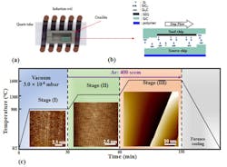
1. Semiconducting epigraphene (SEG) production: (a) Schematic diagram of a CCS furnace with two 3.5- × 4.5-mm SiC chips inside a closed cylindrical graphite crucible that’s supplied with a leak inside a quartz tube. The crucible is inductively heated by high-frequency currents through a coil. (b) The two chips are stacked with the C-face of the bottom chip (Source) facing the Si-face of the top chip (Seed). At high temperatures, a slight temperature difference between the chips causes a net mass flow from the bottom chip to the top chip, resulting in the growth of large terraces on the seed chip by step flow growth on which a uniform SEG film grows. (c) SEG is grown in three stages. In stage (I) in a vacuum, the chip is heated to 900°C for about 25 min. to the surface; stage (II), heating to 1300°C for about 25 min. One bar of argon produces a regular array of bilayer SiC steps and ≈ 0.2-μm-wide terraces. SEG-coated terraces grow in stage (III) at 1600°C in 1 bar of Ar; step bunching and step flow produce large, atomically flat terraces on which a buffer layer grows.
Epitaxial Graphene
The team found that when it was made properly, the epitaxial graphene chemically bonded to the silicon carbide and started to show semiconducting properties. The team's measurements, which were also difficult to make, showed that their graphene semiconductor has 10X greater mobility than silicon.
Their quasi-equilibrium annealing method produced macroscopic atomically flat terraces covered with a well-ordered epigraphene buffer layer that has a 0.6 eV bandgap. Room temperature mobilities exceed 5000 cm2/Vs which is much larger than silicon and 20X larger than the phonon-scattering-imposed limit of current 2D semiconductors. Also critical for nanotechnology, its lattice is aligned with the SiC substrate (Fig. 2).
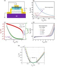
2. (a) Schematic of field-effect transistor with SEG as channel. (b) Transfer characteristics (Ids - Vgs) at bias voltage of 0, 1 and 2 V. (c) Transfer curve of the device at Vds = 1 V and corresponding logarithmic plot. (d) Output characteristic curves of the device. The field effect mobility is μFET = 22 cm2/V-sec. The large reduction compared with the intrinsic SEC properties is caused by scattering from the dielectric and large contact Schottky barriers. (e) Extrapolation of the linear rise of the output curves corresponds well with the bandgap.
The electrical properties of the semiconducting epigraphene (SEG—a well-ordered buffer layer) were measured by characterizing a fabricated top-gated SEG FET. The device exhibits reasonable switching performance with an on/off ratio of ∽104 at Vds = 1 V and Ion = 15 nA.
The threshold voltage (Vth) is −0.21 V, which is extracted by extrapolating the linear regime of the transfer curve to the gate voltage axis. The subthreshold swing (SS) calculated from SS = dVgs/d(logIds) is ∽155 mV/decade. There’s a substantial barrier (SB), which is clear from the nonlinear behavior of Ids at high Vds and the large contact resistances.
The final lattice, aligned with the SiC substrate, is chemically, mechanically, and thermally robust. Moreover, it can be conventionally patterned and seamlessly connected to semimetallic epigraphene, thus making semiconducting epigraphene ideally suited for nanoelectronics. The work is detailed in their paper “Ultrahigh-mobility semiconducting epitaxial graphene on silicon carbide” published in Nature. That posting is behind a paywall, but a preprint is posted here.
Meanwhile, Over in Illinois…
Other researchers are also pursuing the potential of graphene. A joint research effort between the University of Illinois Urbana-Champaign, the National Energy Technology Laboratory (NETL), Oak Ridge National Laboratory (ORNL), and the Taiwan Semiconductor Manufacturing Company (TSMC) is also playing up the attention-getting fact that coal can play a vital role in next-generation electronic devices (is there an impending shortage of silicon?).
The process converts coal char into nanoscale carbon disks called “carbon dots.” The UI research group demonstrated it can be connected to form atomically thin membranes for applications in both two-dimensional transistors and memristors. They used coal-derived carbon layers as the gate dielectric in two-dimensional transistors built on the semimetal graphene or semiconductor molybdenum disulfide to enable more than 2X faster device operating speed with lower energy consumption.
Like other atomically thin materials, the coal-derived carbon layers don’t possess “dangling bonds,” or electrons that aren’t associated with a chemical bond. These sites, which are abundant on the surface of conventional three-dimensional insulators, alter their electrical properties by effectively functioning as “traps,” slowing down the transport of mobile charges and thus the transistor switching speed.
These atomically thin amorphous carbon films are mechanically strong with modulus of 400 ±100 GPa. They also demonstrate robust dielectric properties with high dielectric strength above 20 MV/cm and low leakage current density below 10−4 A/cm. They can be implemented as solution-deposited ultra-thin gate dielectrics in transistors or ion-transport media in memristors, enabling exceptional device performance and spatiotemporal uniformity.
This solution-based process allows for the scalable preparation of amorphous carbon films with thickness down to 1-2 atomic layers covering 3-in. wafers (Fig. 3).
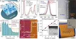
3. (a) Optical image of an atomically thin quasi-2D amorphous carbon film deposited on a 3-in. diameter SiO2/Si wafer. (b) Raman spectra of the carbon-dot assembly as deposited (black dotted line) and after coalescence (red solid line). (c) High-resolution spectrum of the ultra-thin quasi-2D amorphous carbon formed on SiO2/Si substrate (black circles). (d) Reconstructed cross-sectional STEM and (e) associated contrast intensity profile. (f) AFM image of ultra-thin quasi-2D amorphous carbon film patterned to generate an edge by photolithography and oxygen reactive-ion etching. (g) Film thickness as a function of the number of layers deposited. (h) Optical image of an ultra-thin quasi-2D amorphous carbon membrane transferred to a substrate of Au (200 nm)/SiO2 (90 nm)/Si, after immersing in Au etchant. Inset: a magnified view showing an etched pit corresponding to a pin-hole defect in the transferred atomically thin nanomembrane.
This project is detailed in their lengthy paper “Ultrathin quasi-2D amorphous carbon dielectric prepared from solution precursor for nanoelectronics” published in Nature Communications Engineering, along with a complementary lengthy Supplementary information file.
Read more articles in the TechXchange: Distinguishing Discretes.
Reference
1. The Wall Street Journal, “Research in Graphene Shows New Potential for Its Use in Chips.”
About the Author

Bill Schweber
Contributing Editor
Bill Schweber is an electronics engineer who has written three textbooks on electronic communications systems, as well as hundreds of technical articles, opinion columns, and product features. In past roles, he worked as a technical website manager for multiple topic-specific sites for EE Times, as well as both the Executive Editor and Analog Editor at EDN.
At Analog Devices Inc., Bill was in marketing communications (public relations). As a result, he has been on both sides of the technical PR function, presenting company products, stories, and messages to the media and also as the recipient of these.
Prior to the MarCom role at Analog, Bill was associate editor of their respected technical journal and worked in their product marketing and applications engineering groups. Before those roles, he was at Instron Corp., doing hands-on analog- and power-circuit design and systems integration for materials-testing machine controls.
Bill has an MSEE (Univ. of Mass) and BSEE (Columbia Univ.), is a Registered Professional Engineer, and holds an Advanced Class amateur radio license. He has also planned, written, and presented online courses on a variety of engineering topics, including MOSFET basics, ADC selection, and driving LEDs.
Comment About the Article
To join the conversation, and become an exclusive member of Electronic Design, create an account today!

Leaders relevant to this article: