High-Speed Noninverting Summing Amplifier Operates To 220 MHz
Article updated 10/04/22
Chau Tran and Brian Rousseau, Analog Devices, 804 Washburn St., Wilmington, MA 01887
The schematic in Figure 1 is a common summing amplifier with multiple inputs and one single-ended output. It is a variation of a standard inverting amplifier. Point X is a virtual ground and is referred to as the summing junction.
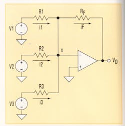
The transfer function for this circuit is:
VO = -[V1(RF/R1) + V2(RF/R2) + V3 (RF/R3)]
This indicates that the output is a weighted sum of the inputs, with the weights being determined by the resistance ratios. If all resistances are equal, the circuit yields the inverted sum of its inputs:
VO = (V1 + V2 + V3)
Note that if the noninverted result, VO = (V1 + V2 + V3), is needed, another inverting amplifier must be added with a gain of −1. The circuit in Figure 1 has many other disadvantages, including low input impedance, different input impedances for positive and negative inputs, narrow bandwidth, and the need for tightly matched resistors.
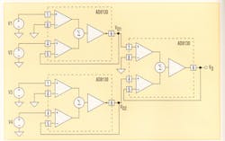
Figure 2 is the schematic of a high-speed summing amplifier, which can sum as many as four input voltages without the need for an inverter to change the sign of the output. This feature can prove useful in audio and video applications. The circuit contains three low-cost, high-speed instrumentation amplifiers. The first two interface with input signals, and their total sum is taken at the third amplifier's output with respect to ground. The in-puts are very high-impedance, and the signal that appears at the network output is noninverting.
Figure 3 is the performance photo at 1 MHz. The top trace is the input signal for all four inputs. The middle trace is the sum of inputs V1 and V2. The bottom trace is the output of the system, which is the total sum of all four inputs.
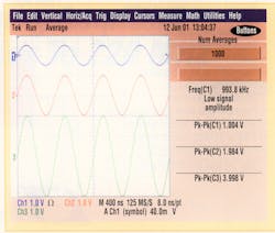
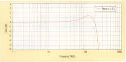
Figure 4 demonstrates the high bandwidth of the system in Figure 2. As can be seen from this figure, the −3-dB point is about 220 MHz.
This article appeared in Electronic Design Oct. 28, 2001.
About the Author
Comment About the Article
To join the conversation, and become an exclusive member of Electronic Design, create an account today!

Leaders relevant to this article: