Synchronizing Multiple ADCs with JESD204B
JESD204B provides a framework for high-speed serial data to be sent along one or more differential signal pairs, such as an output of an analog-to-digital converter (ADC). There's an inherent scheme in the interface to achieve coarse alignment across lanes within the JESD204B specification. Data is partitioned into frames with boundaries that are continuously sent to the receiver.
The JESD204B Subclass 1 interface has provisions for data alignment down to the sample level across multiple serial lane links or multiple ADCs by using a system reference event signal (SYSREF) to synchronize internal framing clocks in both the transmitter and receiver. This creates a deterministic latency for the devices using the JESD204B link. However, there are still many challenges that a system designer must overcome to achieve full timing closure for sampling synchronization, such as PCB layout considerations, matched clock, and SYSREF generation to meet timing, SYSREF periodicity, and digital FIFO delays.
The designer must decide how the device clock and SYSREF signal will be created and distributed throughout the system. Ideally, the device clock and SYSREF should be of the same swing level and offset to prevent inherent skew at the component input pin. The update rate of the SYSREF event will need to be determined as either a single event at startup or a recurring signal that may occur at any time synchronization is needed. Taking the maximum clock and SYSREF signal skew into consideration, careful PCB layout is needed to meet setup-and-hold timing across boards, connectors, backplanes, and various components. Finally, digital FIFO design and signals traversing across multiple clock domains create inherent digital buffer skew within JESD204B transmitters and receivers that must be accounted for and removed in back-end data processing.
System clock generation can come from several sources such as crystals, VCOs, and clock-generation or clock-distribution chips. While the particular system performance will dictate the clocking needs, one must use multiple synchronous ADCs to produce a SYSREF signal that's source synchronous to the input clock. This makes the clock source selection an important consideration in order to be able to latch this system reference event with a known clock edge at a particular point in time. If the SYSREF signal and clock aren't phased-locked, this can't be achieved.
An FPGA can be used to provide a SYSREF event to the system. But unless it also uses and synchronizes to the master sample clock that's sent to the ADCs, it will be difficult to phase-align the SYSREF signal from the FPGA to the clock. An alternate approach is to provide the SYSREF signal from a clock-generation or clock-distribution chip that can phase-align this signal to multiple clocks that are sent throughout the system. Using this method, the SYSREF event can be a one-shot event at startup or a recurring signal depending on the system requirements.
As long as deterministic latency remains constant within the system across ADCs and FPGAs, additional SYSREF pulses may not be needed except to help frame particular system data. Hence, a periodic SYSREF pulse for clock alignment can be ignored or filtered until synchronization is lost. A marker sample for the occurrence of SYSREF could alternately be maintained without resetting the JESD204B link.
To initiate a known deterministic starting point for the ADC channels, the system engineer must be able to close timing for the SYSREF event signal distributed across the system. The expected setup-and-hold time relative to the clock then must be met without violation. A relatively long SYSREF pulse that spans multiple clock cycles can be used to meet the hold time requirement, so long as the setup time to the first required clock can also be met.
Managing Skew
Careful attention to PCB layout is critical in this effort to maintain matched trace lengths for clocks and SYSREF within the system for minimum skew. This may be the most difficult part of achieving synchronous sampling processing across channels. The effort will only get progressively more challenging as ADC encode clock rates increase and multi-board systems become more complex.
SYSREF to clock board skew at components across boards and connectors must be deterministically known for each device by the system engineer. Any remaining inter-device digital and clock skew delays need to be effectively nulled in the FPGA or ASIC. Back-end processing can change the sample order across ADCs and introduce any needed realignment to prepare the data for further synchronized processing.
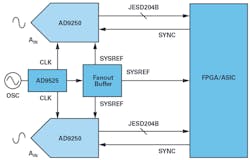
Inter-device sample skew can be corrected by delaying the fastest data samples and transmitter latency to align with the slowest data samples in the back-end FPGA or ASIC. For complex systems, this may involve multiple FPGAs or ASICs where each needs to communicate its total inter-device sample latency for final alignment. By introducing appropriate elastic buffer delays in the JESD204B receiver(s) to accommodate each specific transmitter latency delay, the inter-device sample skews can be aligned with known determinism across a system (see figure).
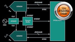
Multiple ADCs can be synchronized using a source synchronous SYSREF and clock generator with fan-out buffer to meet digital input timing requirements. An FPGA can adjust for SERDES skew with digital buffers to align samples.
The AD9250 is a 250-Msample/s, 14-bit dual ADC from Analog Devices that supports the JESD204B interface in a Subclass 1 implementation. This subclass allows for analog sample synchronization across ADCs using the SYSREF event signal. The AD9525 is a low-jitter clock generator that not only provides seven clock outputs up to 3.1 GHz, it also can synchronize a SYSREF output signal based on user configurations. These two products, coupled with a selection of fanout buffer products from Analog Devices, provide the framework to accurately synchronize and align multiple ADC data sent to an FPGA or ASIC for processing.
Ian Beavers is a product engineering manager for the Automation Energy and Sensors Team located at Analog Devices, Greensboro, NC.
About the Author
Ian Beavers
Product Engineering Manager, Automation Energy and Sensors, Analog Devices
Ian Beavers is a product engineering manager for the Automation Energy and Sensors Team located at Analog Devices, Greensboro, N.C. He has worked for the company since 1999. Ian has over 20 years of experience in the semiconductor industry. He earned a bachelor’s degree in electrical engineering from North Carolina State University and an M.B.A. from the University of North Carolina at Greensboro.
Voice Your Opinion!
To join the conversation, and become an exclusive member of Electronic Design, create an account today!

Leaders relevant to this article:

