Op Amps Make Precision Clipper, Protect ADC
This file type includes high-resolution graphics and schematics when applicable.
It can be a challenge to match the voltage range of an analog signal to the input range of an analog-to-digital converter (ADC). Exceeding the ADC’s input range will give an incorrect reading. And if the input goes far enough beyond the power-supply rails, substrate currents may flow into the ADC, which can then cause latch up or even damage to the part. However, restricting the input-voltage range to lower, more-conservative levels wastes the ADC’s dynamic range and resolution.
A simple op-amp clipper (Fig. 1) prevents these problems. The maximum allowable input voltage is applied to the non-inverting input of U1, and the output is fed back to the inverting input via small-signal diode D1. The ADC’s reference voltage can be used for the clipping reference if available. When the input voltage is below the reference, U1’s output is driven to the positive rail and D1 is reverse-biased, so the input signal passes through without being altered.
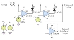
When the input goes above the clamp voltage, the op-amp output reverses and closes the loop through D1. As a result, it effectively becomes a unity-gain follower to the clamp voltage. Input resistor R1 limits the amount of current the op-amp output has to sink. A second op amp (U2) performs the complementary negative clipping function, preventing the signal from going below ground. Thus, in this example, the output signal is restricted to 4.096 V to 0 V out.
While simple in concept, this circuit poses unique challenges for the op amp. First, most modern op amps have back-to-back diodes across their input to prevent the application of large differential voltages to the inputs. This can cause damage to the part or shifts in the input offset voltage. In this circuit, these diodes would prevent the output signal from going more than one diode drop below the positive clamp voltage or one diode drop above the negative clamp voltage.
Deciding whether a given op amp has these diodes can require some detective work. Some parts’ datasheets show the presence of the input diodes, but others don’t. Another indication of the diodes’ presence is a limitation in the Absolute Maximum Ratings section of input current to a few milliamps.
In addition, the output of the op amp has to slew from the “unclamped” to the “clamped” state as quickly as possible in order to clamp a fast-rising signal without a potentially dangerous overshoot. Furthermore, rail-to-rail input and output operation of the op amp is desired so it can function with voltages close to the limits of the power supplies.
The LT6015 family of op amps, which includes the LT6016 dual and LT6017 quad versions, addresses these issues. Because there are no diodes on the inputs, they can have a very large differential voltage, which should not impose a limitation on any practical ADC application. Use of large differential voltages at the input allows the introduction of clamping and other nonlinear circuits. Furthermore, the input voltage can go as high as 80 V above or 25 V below the V– rail, which allows the part to survive inputs that would damage other parts.
The LT6015 is further unique in that it allows a power-supply range from V+ to V– of up to 60 V, which would allow use of the circuit to clamp higher voltages than the great majority of op amps. It also has a slew rate of 0.75 V/µs, which enables it to clamp reasonably fast-rising signals. The sub-100-µV typical offset voltage ensures that the clamping level is very accurate.

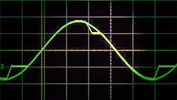
Figure 2 shows the LT6015 driven from ±10-V supplies clamping a 7-V p-p, 1-kHz sine wave at 0 V and 4 V. It’s hard to see the clamping action, but if you zoom in on the output, you can see a small overshoot (Fig. 3).
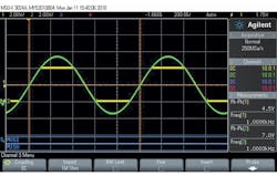
Increasing the input frequency to 30 kHz (Fig. 4) clearly shows the clamping action taking place in less than 10 µs, limiting the operating bandwidth of the circuit to a few kilohertz. The clamping speed can also be increased by limiting the voltage-supply rails to close to the clamping-limit voltages, which lowers the voltage range that the output must slew to go into clamping mode. Since the LT6015 output swings very close to the supply rails, little extra voltage range is needed.

Another limitation on this circuit is that the output resistance is defined by R1, which needs to be at least a few hundred ohms to limit the output of current in the op-amp output. Since some ADCs need to be driven by a low resistance, buffer amp U3 might be required. Using the LT6017 quad-version package would permit a single part to perform all of these functions.
Thomas Mosteller has been a Field Applications Engineer for Linear Technology’s Middle Atlantic region since 1990. He has assisted a wide range of military, commercial, and industrial customers with designs in many fields, such as power distribution and supplies, analog signal conditioning, data conversion, and RF and communications applications. Prior to joining Linear Technology, Thomas designed medical equipment for 10 years, and holds a patent in the design of infusion pumps. He earned a BSEE from Drexel University in 1977.
Aaron Schultz is an applications engineering manager at Linear Technology. Aaron has worked for 20 years at the chip and system level in design and applications, in fields including solid-state lighting, photovoltaics, multiphase dc-dc and other power-conversion topics, high-speed data communications, fiber optics, and high-speed memory. His schooling includes Carnegie Mellon University (’93) and MIT (’95). By night he plays jazz piano.
Looking for parts? Go to SourceESB.
This file type includes high-resolution graphics and schematics when applicable.
About the Author
Aaron Schultz
Applications Engineering Manager
Aaron Schultz is an applications engineering manager whose multiple system engineering roles in both design and applications have exposed him to topics ranging across battery management, photovoltaics, dimmable LED drive circuits, low voltage and high current dc-to-dc conversion, high-speed fiber-optic communication, advanced DDR3 memory R&D, custom tool development, validation, and basic analog circuits, while over half of his career has been spent in power conversion. He graduated from Carnegie Mellon University in 1993 and MIT in 1995. By night he plays jazz piano.
Thomas Mosteller
Thomas Mosteller was a field-applications engineer for Analog Devices’s Mid-Atlantic region starting in 1990. He assisted a wide range of military, commercial, and industrial customers with designs in many fields such as power distribution and supplies, analog signal conditioning, data conversion, and RF and communications applications. Prior to joining Linear Technology (now Analog Devices), Thomas designed a wide range of medical equipment for 10 years and holds a patent in the design of infusion pumps. He earned a BSEE from Drexel University in 1977.
Comment About the Article
To join the conversation, and become an exclusive member of Electronic Design, create an account today!

Leaders relevant to this article: