Simple Change Enhances Safety, Integrity of Isolated Shunt-Regulator DC-DC Converter
This file type includes high-resolution graphics and schematics when applicable.
Did you know that your shunt regulator is in danger? Don’t worry—the fix is free (and free is good).
A feedback circuit commonly used in isolated dc-dc converter applications uses a shunt regulator (such as the ATL431) and an optical isolator to feed the output voltage back to the pulse-width-modulator (PWM) controller. This circuit is effective and easy to use. However, few designers are aware of the hidden electrostatic discharge (ESD)/electrical overstress (EOS) danger this poses.
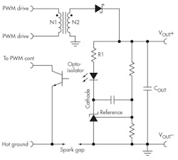
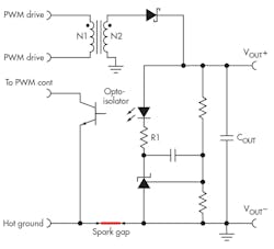
At first glance, the shunt regulator in Figure 1 seems immune to EOS. An overvoltage on VOUT will cause the cathode voltage to drop and the reference pin will not rise due to the internal diode from the reference pin to the cathode pin. The series resistors will protect the shunt by limiting the current on both the reference and cathode pins. A negative voltage VOUT will not hurt the shunt, due to the rectifier clamping the voltage and the series resistors limiting current to the shunt.
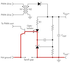
However, the shunt regulator can be damaged if the voltage across the isolation becomes too high during an ESD event. The weakest point in the isolation is usually the opto-isolator leads. Once the opto-isolator gap is breached, the easiest path for ESD discharge will be though the shunt regulator, as shown by red line in Figure 2.
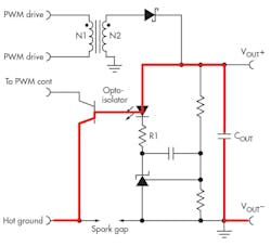
Moving resistor R1 from the anode of the opto-isolator to the cathode side will protect the shunt during an isolation breach. Moving the resistor has no effect on performance or stability. It works because the opto-isolator breach will now prefer the output capacitor as a path to ground. The red line in Figure 3 shows the new ESD path.
Since the shunt regulator is no longer in the primary ESD path, it will survive. The capacitor now takes the current, but it will tolerate much higher ESD energies than the shunt regulator. Depending on which pins on the opto-isolator pass the electric arc, there will still be significant danger to the PWM controller and some danger to the opto-isolator itself.
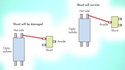
Another danger can occur in space-constrained designs. If the shunt or its node traces are placed too close to the isolated (hot ground) traces, there’s a chance that an electric arc can occur directly to the shunt or its circuit traces (Fig. 4). In this case, moving R1 will not protect the shunt. The solution is to rotate the shunt so that the anode (ground) is the closest node to the traces on the other side of the isolation gap.
For additional protection, you can add an intentional spark gap to cause an ESD event to arc from the ground of one side to the ground of the other side. The spark gap will need a substantially lower breakdown voltage to ensure that the arc doesn’t choose an alternate place to cross. It’s clear from Figure 5 that an arc across a spark gap will not stress the components.
Simple changes can greatly improve ESD performance—and as promised, these changes are free.
Ronald Michallick, a linear applications engineer at Texas Instruments, provides application support for standard linear devices. Ron has nearly two decades of engineering experience, is credited with three patents, and is a graduate of ITT Technical Institute in Tampa, Florida. You can reach him at https://e2e.ti.com/members/11001/
Reference:
“Understanding Voltage References,” (TI E2E Community Blog Forum)
About the Author
Ron Michallik
Linear Applications Engineer
Ronald Michallick, a linear applications engineer at Texas Instruments, provides application support for standard linear devices. Ron has nearly two decades of engineering experience, is credited with three patents, and is a graduate of ITT Technical Institute in Tampa, Florida. You can reach him at https://e2e.ti.com/members/11001/
Voice Your Opinion!
To join the conversation, and become an exclusive member of Electronic Design, create an account today!

Leaders relevant to this article:
