Flip-Flop Design Provides Frame Sync for Received Satellite Telemetry
This file type includes high-resolution graphics and schematics when applicable.
Satellite-telemetry data is digitized, multiplexed, and formatted into frames at a 1-kb/s data rate typically, and transmitted on a downlink frequency using data formats such as shown in the table.1-3
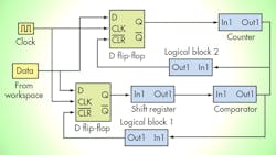
The telemetry data is transmitted using a multilevel-modulation technique, usually via phase-shift keying/phase modulation (PSK/PM) to overcome the effects of phase noise. After the signal is received, demodulated, and decoded at the ground station, frame synchronization is needed to extract the telemetry parameters and obtain the data. This can be done with a simple circuit built almost entirely with flip-flops. Fig. 1 shows the overall block schematic as represented in MathWorks' Simulink.
Each frame consists of a frame-synchronization sequence of 24 bits (assumed to be hex “ACCA1F” in the example here) followed by 125 words of 8-bit length representing the data. The main circuit contains two D flip-flops, D1 and D2, which act as switches to send and stop the data flow into following circuit. The output of the D1 is fed to a 24-bit serial-in, parallel-out (SIPO) shift register that’s synchronized with the generated clock.
At each clock transition, the data clocks into the flip-flop’s bank (shift register). After 24 clock pulses, the first 24 received bits are taken inside the shift register and the parallel outputs are fed to a comparator connected to the output of the shift register. The comparator is a single-bit implementation where each output of the shift register is connected to 24 comparators and compared with the 24 bits of the frame-sync code ACCA1F.
The data keeps entering the shift register until the frame sync is matched. Once matched, the comparator output goes high, which changes the state of D1 to stop the flow of data into the shift registers. At the same time, D2 (which was inactive during this period) is enabled by the comparator output. The data that comes after the 24 bits is routed through D2 to a 10-bit counter that’s configured as a 1000-bit counter with Simulink model (Fig. 2), and which counts the clock pulses from the instant data starts flowing out of D2.
2. The Simulink model of the frequency counter shows the 10 D-type flip-flops that implement the counting function. (Click image to enlarge)
Once the 1000-count is reached, the counter resets the operation to initial condition by disabling D2 and enabling D1, which sends the subsequent data bits into the shift registers to detect frame sync of the next frame. The cycle repeats as the data keeps coming. The output of D2 is stripped out for every eight bits and displayed.
The shift-register block contains the cascade of the 24 D-type flip-flops. The data is input to the first flip-flop and the output of the flip-flop is the input to the second flip-flop, and so on. This cascade connection implements the SIPO shift register. The comparator is a combinational circuit of logic gates that checks for the condition of A = B, where A and B are single-bit inputs. The 24 constant bits of the frame sync are the reference inputs (A) to the 24 comparators, while the 24 shift-register outputs are second (B) inputs.
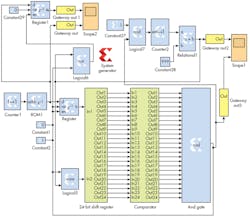
3. The System Generator Model uses the Xilinx XUPV5-LX110T FPGA Board and associated System Generator Software tool. (Click image to enlarge)
The system is implemented on the Xilinx XUPV5-LX110T FPGA Board4 using the System Generator Software tool, also from Xilinx, with the system-generator circuit shown in Fig. 3. The data format contains bits corresponding to ACCA1F in the first 24 bits. Thus, the output of D2 for the first 24 pulses is zero, and then the 1000 bits (125 words) of data are obtained from the 25th clock pulse onwards, until the comparator output goes high.
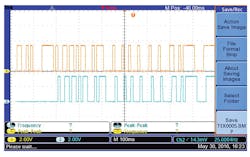
Figure 4 shows the received data (upper trace) and the data at the output of D2 (lower trace). The output is zero until it matches the frame sync, then the next 1000 bits are matched with the input data stream. These data bits are processed to separate the words, and each word data is decoded and displayed in engineering units for the user.
Acknowledgement: The authors would like to thank Dr. K.N.B.Murthy, Vice Chancellor, Dr. T.S.Chander, Chairperson, Electronics and Communication Dept., and Dr. V.K. Agrawal, Director, CORI, PES University for the encouragement which they provided.
Nithin Kumar was a student with an under-graduation degree of Bachelors in Telecommunication; Chirag R was a student with an undergraduate degree of Bachelors in Telecommunication; and Dr. V Sambasiva Rao is a professor at Department of Electronics and Communication with Satellite Technologies as his major area of research. All work at PES Institute of Technology.
References
1. Consultative Committee for Space Data Systems (CCSDS) Green Book, CCSDS 100.0-g-1, December 1987.
2. D.V. Raju, R.K. Rajangam, P.S. Rajyalakshmi, “The Telemetry System,” Proceedings of Indian Academy of Science, Volume C1, No.2, September 1978, pages 184-198.
3. S.N. Prasad and S. Pal, “Telemetry, Tracking and Command Systems of Spacecraft,”IETE Technical Review, Volume 20, Issue 6, 2003.
4. Xilinx User Guide, ML505/ML506/ML507 Evaluation Platform, UG347 (v3.1.2), May 15, 2011.
About the Author
Nithin Kumar K
Chirag R
Voice Your Opinion!
To join the conversation, and become an exclusive member of Electronic Design, create an account today!

Leaders relevant to this article:


