Understanding an Instrument Amplifier’s Linear Operating Range
This file type includes high-resolution graphics and schematics when applicable.
Instrument amplifiers (INAs) are widely used for signal conditioning in data-acquisition systems and telemetry. Their differential inputs, high input impedance, and high gain make them ideal candidates for boosting the output of low-amplitude sensors like thermocouples and strain gauges. This article explains the linear operating region of an INA and how it’s defined by the common-mode input voltage and the output-voltage plot.
Instrument Amplifier Basics
Most instrument amplifiers consist of three op amps connected as shown in Figure 1. Amps 1 and 2 provide gain and high input impedance, while Amp 3 is a differential amplifier. These op amps are typically packaged along with the resistors in a single IC.
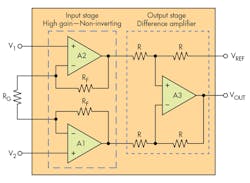
All of the differential-amp resistors are usually the same value, giving this stage a gain of 1. The input stage uses feedback resistors RF and input resistor RG. The gain set resistor RG is external to the IC. The gain is determined by the expression:
A = (2RF/RG) +1
The output is computed with the expression:
VOUT = A(V2 – V1) + VREF
V1 and V2 are the input voltages. VREF is used to center the output if there’s a single supply.
Making RG small compared to RF gives a very high gain, making it possible to measure microvolt and millivolt sensor signals. A gain of 1000 or more is typical.
The common-mode rejection ratio (CMRR) reveals how well common-mode signals are cancelled. CMRR is defined as the ratio of the differential gain A to the common mode gain ACM:A key feature of an INA is its differential configuration, which is instrumental in cancelling noise or other unwanted signals that are common to the two inputs. A frequent problem involves 50-/60-Hz noise that radiates from power lines and is coupled into both input lines. This common mode signal is effectively subtracted out so that it doesn’t interfere with any low level signals on the input lines.
CMRR = A/ACM
The common-mode rejection (CMR) of the amplifier is usually expressed in decibels:
CMRR = 20log(CMRR)
Most quality INAs have a CMR in the 80- to 130-dB range. The quality of the amplifier depends on how well the input amplifiers are matched and the precision of the internal resistors on the differential amplifier. A resistor tolerance of 0.01% or better is required for a high CMRR.
CMRR is typically stated assuming dc inputs. With ac inputs, the CMRR decreases with frequency as capacitance and other parasitics begin to affect the balances in the circuits.
Understanding VCM vs. VOUT Plots
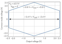
The most common issue when working with instrumentation amplifiers involves the VCM vs. VOUT plot, which defines the linear operating region of the device (Fig. 2).
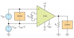
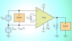
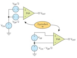
This plot is developed with the measurement arrangement shown in Figure 3, which requires two precision voltage sources and two accurate digital multimeters (DMMs). The differential voltage Vdif is defined as:
VDIF = V2 – V1
The common-mode voltage VCM is defined as:
VCM = VCM – VDIF/2
The reason for the VDIF/2 factor in the equation is due to the difference between the mathematical analysis model and the more practical measurement arrangement in Figure 3 with VCM connected to one input. The mathematical model usually represents VDIF as two sources equal to VDIF/2 (Fig. 4). The two models are equivalent.
Referring to Fig. 2 and assuming ±2.5-V supplies on the INA, notice that the full output swing of ±2.4 V is only available when the common-mode voltage is zero. With a 2-V common-mode voltage, the output swing is limited to ±0.8 V.
Reference Design
Texas Instruments offers a reference design that uses its INA333 instrument amplifier and a strain-gauge bridge. The main supply is 5 V in a single-supply arrangement with a 2.5-V reference (VREF) input to center the output between the rails when the input is zero (Fig. 5). The bridge supply is also 2.5 V. R1, R2, and R3 are usually set equal to RSG, the strain gauge resistance, which is typically 120 Ω. Resistors R4 and R5 set the bridge current and the common-mode inputs of the instrument amplifier.
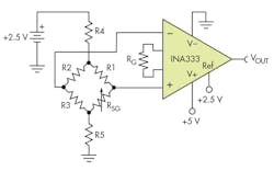
This strain-gauge reference design accurately measures the resistance of a strain gauge by being placed in a bridge configuration. The reference design includes theory, complete error analysis, component selection, simulation, PCB design, and measured data that correlates with theory, calculations, and simulation.

About the Author

Lou Frenzel
Technical Contributing Editor
Lou Frenzel is a Contributing Technology Editor for Electronic Design Magazine where he writes articles and the blog Communique and other online material on the wireless, networking, and communications sectors. Lou interviews executives and engineers, attends conferences, and researches multiple areas. Lou has been writing in some capacity for ED since 2000.
Lou has 25+ years experience in the electronics industry as an engineer and manager. He has held VP level positions with Heathkit, McGraw Hill, and has 9 years of college teaching experience. Lou holds a bachelor’s degree from the University of Houston and a master’s degree from the University of Maryland. He is author of 28 books on computer and electronic subjects and lives in Bulverde, TX with his wife Joan. His website is www.loufrenzel.com.
Comment About the Article
To join the conversation, and become an exclusive member of Electronic Design, create an account today!

Leaders relevant to this article: