How to Boost Performance in Synchronous Buck Converter Designs

Download this article in PDF format.
The synchronous buck converter is a widely used topology in low-voltage, high-current applications. One common application is a point-of-load (POL) converter that transforms a system bus voltage of 48 V, say, to 1 V or below to power high-performance microprocessors, FPGAs, or ASICs.
Figure 1 shows the schematic of a synchronous buck converter. The circuit replaces the diode in the basic buck circuit with a low-side (LS) FET chosen for low RDS(ON). The FET costs more than a diode, but enhances converter efficiency. Learn more about synchronous versus nonsynchronous buck converters here.
Synchronous buck designs can achieve efficiencies over 90%. At these levels, improving performance requires both a good understanding of the sources of power loss and a fanatical dedication to reducing them further.
An ideal switching converter, or course, has zero power losses. When an ideal power switch is open, it has infinite resistance; thus, the current through it is zero. When the switch is closed, it has zero resistance, so the voltage across it is zero. In both states, there’s zero power loss; the switch also switches between the two states in zero time.
Other components also exhibit ideal characteristics. Inductors have zero resistance and capacitance, printed-circuit-board (PCB) traces and leads have no resistance or parasitics, and so on.
Real devices aren’t so accommodating. A synchronous buck converter has MOSFET losses, inductor losses, and PCB losses, among others. Let’s examine some of the losses associated with the switching MOSFETs and drive circuitry. A good discussion of losses and power-supply efficiency can be found in Texas Instruments’ Analog Applications Journal.
Conduction Losses
Unlike an ideal switch, a MOSFET has a non-zero resistance across it when fully on, so it dissipates power—described as conduction loss—as current flows through the device. The datasheet describes the resistive parameter as on-resistance, or RDS(ON).
The conduction loss is independent of switching frequency. Total conduction loss in the circuit of Figure 1 is the sum of the high-side (HS) and low-side (LS) FET conduction losses, plus minor losses due to the FET gate drivers.
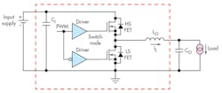
1. A synchronous buck converter sacrifices cost for increased efficiency by replacing the freewheeling diode with a low-side FET. (Source: Texas Instruments)
The conduction losses are inversely proportional to the size of the MOSFET; a larger switching transistor has a lower RDS(ON) and, therefore, a lower conduction loss. On the other hand, a larger MOSFET also has larger parasitic capacitances that increase switching losses, which is discussed next.
Switching Losses
A real-world MOSFET has a finite switching time between the OFF and ON states. That’s because it has parasitic gate-to-source capacitance (CGS) and gate-to-drain capacitance (CGD), both of which must be charged during turn-on and discharged during turn-off. While the FET is switching between states, it’s subjected to both high current and high voltage, which cause switching loss.
Figure 2 shows an idealized representation of the voltages and currents during HS FET turn-on. Applying a voltage to the gate pin supplies gate current (IG), which is calculated as C(dV/dt), and begins charging the internal capacitors of the FET.
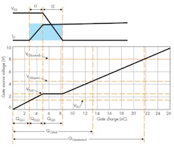
2. These represent ideal waveforms during HS FET turn-on. (Image Source: Texas Instruments)
As the capacitors charge, VGS rises. When charge QGS1 has been supplied, VGS reaches the threshold voltage (VTH) and drain current (IDS) begins to flow. After QGS1 + QGS2 has been supplied, IDS reaches its maximum value, and VDS begins to decline. The driver must supply an additional QGD charge before VDS reaches zero and the FET is fully on.
The total time to supply (QGS2 + QGD)—i.e., the time between fully off and fully on—is t1 + t2, and switching loss occurs during this time. The FET switching losses are a function of load current (IOUT) and the switching frequency (fSW), as shown by:
PSW = VDS x ID x fSW x [(QGS2 + QGD)/IG]
where QGS2 and QGD depend on the amount of time needed to charge the FET.
A similar analysis applies to turn-off. The total HS FET switching loss is the sum of the turn-on and turn-off losses.
The switching losses for the complete synchronous buck include contributions from the HS and LS FETs, their gate drives, the FET output capacitance loss, and a loss due to the LS body diode, which conducts the load current during the required “dead time” when both FETs are off. This application report discusses the various losses in more detail.
Once again, there’s a tradeoff to consider: The switching loss increases linearly with switching frequency, but a higher switching frequency also improves transient response time and decreases the size of the design by allowing the use of smaller inductors and capacitors.
Common-Source Inductance and Efficiency
Fundamental properties of the semiconductor die are responsible for the losses discussed above, but other circuit elements play a role, too.
Parasitic inductances can slow down the turn-on and turn-off time of the FET and increase switching losses. The FET package bond wires and PCB traces are both sources of parasitic inductance.
Figure 3 shows the internal and external inductances in the source path of the HS FET: Their sum is shown as LCSI, the common source inductance (CSI). Both the drain-source current and the gate-charging current flow through LCSI.
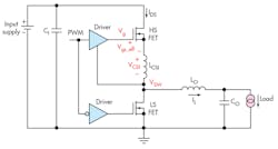
3. The common source inductance (LCSI) includes both internal and external inductances. It contributes to switching losses by increasing both turn-on and turn-off times. (Source: Texas Instruments)
Any change in the drain source current will induce an opposing voltage (VCSI) across the common-source inductance (LCSI):
VCSI = LCSI × (dIDS/dt)
This voltage will actively modify the gate source voltage of the power MOSFET. The effect will be more significant during turn-on and turn-off when IDS and Vgs are changing quickly. The effective gate-source voltage is reduced by VCSI as given by:
Vgs_eff = Vg ‒ VSW ‒ VCSI
By reducing the value of VGS seen by the FET, the common source inductance acts to increase the turn-on and turn-off times. The result is increased switching loss.
Process and Packaging Improvements to Increase Efficiency
Several disciplines can contribute to reducing power losses and thereby improve the efficiency of a synchronous buck converter.
In semiconductor technology, enhancement efforts have been underway for decades; power MOSFETs have steadily improved since they first appeared in the 1970s. The widely used TrenchFET technology now offers much lower RDS(ON) than first-generation DMOS devices. The low resistance reduces the conduction loss, but parasitic capacitances remain, so switching losses are still an issue.
NexFET, Texas Instruments’ third-generation macrocell power MOSFET technology, reduces the parasitic capacitances by about 50% compared to TrenchFET, while offering comparable RDS(ON). Lower capacitances mean lower input gate charge and shorter voltage transients during switching, enabling an increase in the operating frequency. You can read more about FET technology and the development of NexFET here.
Improved packaging and layout are required to reduce CSI. Multichip modules pack the devices closer together and reduce trace lengths, but still require internal bond wires. These designs place components side-by-side and are restricted to two dimensions. However, new packages using Texas Instruments’ PowerStack technology are placing components on top of each other in a three-dimensional arrangement.
4. Due to the vertical nature of the NexFET design, two devices can be stacked in a three-dimensional PowerBlock package. (Source: Texas Instruments)
Three-dimensional packaging has several electrical and thermal performance benefits if the individual components are suitable. In a synchronous buck converter configuration, the NexFET's vertical current flow makes it ideal for stacking. In a three-dimensional package, the high-side FET source terminal is located directly above the low-side FET drain terminal, virtually eliminating resistance and parasitic inductance between the devices and allowing faster switching. The source terminal of the low-side FET is at ground potential and attached to the exposed pad of the package for highly efficient heat transfer.
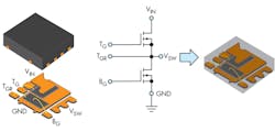
Figure 4 shows the configuration of a high-side and low-side NexFET pair in a PowerBlock package. The high-side FET drain (VIN) and the switching node (VSW) are high-current connections. These are attached to the pins with clip-bonding technology that replaces the traditional wire-bond connection with a solid copper bridge. Clip bonding substantially reduces RDS(ON) and conduction losses compared to wire bonding.
Removing the bond wires and PCB traces between the HS FET source and the HS FET drain also pays dividends in cutting LCSI to <100 pH (Fig. 5).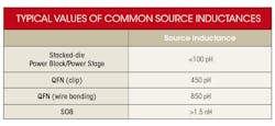
5. The CSI can vary widely between packages. (Source: Texas Instruments)
TI offers 14 different footprint-compatible power blocks optimized for different currents and duty cycles. These come in two small outline no-lead (SON) packages: 3 × 3 mm or 5 × 6 mm. The packages feature a large lead frame that provides the ground connection for the low-side MOSFET. The use of multiple thermal vias to pull heat from the package provides excellent thermal performance.
PowerBlock Efficiency Improvements
The lower common-source inductance of the PowerBlock package leads to improvements in converter efficiency. For example, the CSD87350Q5D NexFET half-bridge power block is designed for synchronous buck applications. When paired with external 5-V gate drivers, it features high-current, high-efficiency, and high-frequency capability in a 5- × 6-mm package.
Figure 6 shows the efficiency of a synchronous buck converter with the CSD87350Q5D compared to the same design with discrete power FETs. The PowerBlock design gives a 2% efficiency improvement in all but light load conditions.
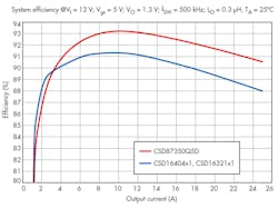
6. The CSD87350Q5D PowerBlock has superior efficiency compared to the same design with two discrete NexFETs (Source: Texas Instruments)
The new PowerBlock II system, used in products like the CSD87381P, allows for cooling from both the top and bottom of the package. That’s because it offers the ability to add a heat sink.
Conclusion
Improving the performance of high-efficiency synchronous buck converters requires identifying every source of power loss and minimizing its contribution.
Success takes a multi-disciplinary approach, combining state-of-the-art MOSFETs with innovative power packaging designs. TI’s PowerBlock devices fit the bill and help designers extract a little more performance out of a topology that is already highly efficient.

About the Author
Paul Pickering
Paul Pickering has over 35 years of engineering and marketing experience, including stints in automotive electronics, precision analog, power semiconductors, flight simulation and robotics. Originally from the North-East of England, he has lived and worked in Europe, the US, and Japan. He has a B.Sc. (Hons) in Physics & Electronics from Royal Holloway College, University of London, and has done graduate work at Tulsa University. In his spare time, he plays and teaches the guitar in the Phoenix, Ariz. area
Comment About the Article
To join the conversation, and become an exclusive member of Electronic Design, create an account today!

Leaders relevant to this article: