
Download this article in PDF format.
Back in 2010, Bob Pease sent me a couple pictures of some prototype printed circuit boards (PCBs) he had made in the early 1960s. Pease got to be a great analog engineer because he would hack away at circuits, working with his hands and real parts, instead of computer simulations. Pease wrote:
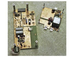
“The first photo (Fig. 1) looks like a typical P45-type discrete-component Philbrick op-amp from the 1963-1970 era. We had some excellent performance, in small packages. If you didn't have a suspicious eye, you'd say, OK, big deal, it's a fair layout.
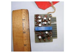
1. Bob Pease made this prototype of the Philbrick P45 op amp back in the 1960s. The top-side of the board looks like a production PCB.
“The reverse view in the second photo (Fig. 2) shows how we did it, a classical pseudo-PCB layout. There are many small foils, and several long buses. That's how we liked to do it. We did this to represent that this was a feasible circuit, and we could plug it in and evaluate the circuit in a user's system. Yet from the top, it looks just like a real PCB layout. If we were in a big hurry, we could go forward from the pseudo-PCB layout to a real PC board in a couple days. / rap”
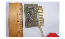
2. The bottom of the Pease prototype shows how the leads connect to serve as traces. It’s possible to change and rework components, but not easy.
I love that link to the P45 op amp, since it shows the actual production board. You can see the similarities to Pease’s prototype. Pease was known for his “airball” prototypes; he soldered together leaded components in the air. It was OK for low-frequency circuits.
An “airball” is not very conducive to putting things into production. I always prefer to get a real circuit board as soon as possible. Even if it just brings power to the chips, it mounts them firmly, and you can cut and jump and hack on them much like an “airball” prototype. You can also “dead bug” on a PCB, where you glue a chip with its leads pointing upwards and then connect to the leads with wires and discrete components. So-called “Manhattan-style” dead-bugging even lets you prototype RF circuits.
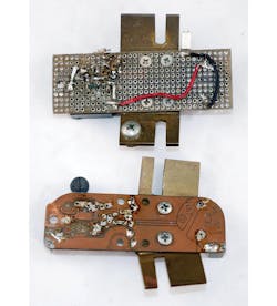
3. Prototypes for a Harley generator voltage regulator use pegboard (top) and home-etched (bottom) prototyping methods.
Looking in my drawer of old prototypes, I found two early attempts at a generator-mounted voltage regulator for my Harley Sportsters (Fig. 3). I started out using plated “pegboard” PCB material. It has holes on tenth-inch centers, with a solder pad on both sides. The holes are plated-though like a production PCB. It worked pretty well in the days of leaded components and DIP (dual-inline plastic) ICs with tenth-inch centers. I definitely prefer it to original Vectorbord®, which has the holes but no solder pads. Vector also sells the plated-through boards, as well as boards with pads on one or both sides but with unplated holes.
DIY PCBs
After I grew weary of trying to connect all of the leads on a pegboard, I started to etch my own PCBs. First, you buy copper-clad material that has photoresist on one or both sides. Next design the layout backwards, where the lines are creating copper islands, similar to what a PCB milling machine must do. I used AutoCAD for this. Then print out the layout on clear transparency film. You use that to mask off the PCB and expose it to light. Then drop the PCB into a dish of ferric-chloride etchant, preferably heated on a hot-plate.
You can drill a couple of holes in the pre-sensitized PCB material to serve as registration marks for the transparency film. That way, you can make two-sided PCBs at home. Unfortunately the holes won’t be plated through. You soon learn to never put vias under a component. That makes it tough to solder a jumper wire in the via hole.

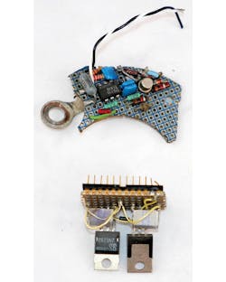
4. The top-sides of the prototype Harley voltage regulators mount components like production PCBs. Both methods allow the hacking in of changes and new components.
Like the Pease prototypes, these methods look similar to a production PCB from the top (Fig. 4). What these methods give you is the same component placement as a production PCB. That helps you check clearances, especially upwards clearance. It’s easy to forget about the Z-axis when working a 2D CAD (computer-aided design) program.
The pegboard prototype could make compact circuits back in the through-hole component days (Fig. 5). It also could serve as a way to mount a little prototype on one of those DIP-style prototyping component carriers. This allows you to make a whole series of circuits that are in easily replaceable modules. Those can go in a wirewrap motherboard. You can also use a larger sheet of pegboard to mount sockets that take the modules.
5. Pegboard construction allowed tight circuit layout back in the through-hole component days (top). You can solder a pegboard prototype into a component carrier to make a little module (bottom).
Besides pre-sensitized photoresist copper-clad, you can use toner-transfer methods to put traces on plain copper-clad PCB material. Your printer toner becomes the PCB traces when you print it on special toner-transfer film. You heat the film as you press it to the copper-clad. The toner then transfers off the film and onto the PCB. It is slick, but shares the problem of no plated-through holes. Still, one nice thing about both home-brew methods is that you can make boards with large copper areas that serve as ground planes (Fig. 6).
6. Home-etched PCBs can have large ground planes on one side. These switching power-supply prototypes have better performance and lower noise than airball prototypes. They also let you evaluate creepage and clearance distances before going into production.
Dealing with Those Surface-Mounts
Modern components are surface-mount. That can make them hard to prototype. One solution is to use adapter boards and demo boards (Fig. 7). Adapter boards mount tiny surface-mount components and bring them out to larger pin spacing, often the same tenth-inch spacing of pegboards and traditional through-hole PCBs.
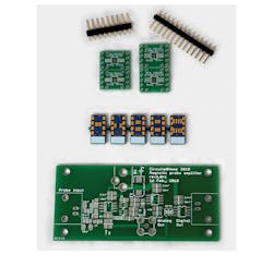
7. Adapter boards and demo boards let you use surface-mount components. Schmartboard makes PCBs with extra-thick soldermask (top). This makes it easy to solder in tiny surface mount components without a microscope or fancy soldering iron. Alan Martin at Texas Instruments made up adapter boards to give DIP spacing to tiny components (middle). The folks at Circuits@Home made a Jim Williams design into a PCB (bottom). You can use it standalone or solder it into a bigger breadboard.
A demo board can serve as a great circuit element that you dead-bug or hack into your prototype PCB. Some demo boards are designed to plug into standard systems, such as Arduino Shield PCBs. I have engineer pals who design their own prototype PCBs, which they can use to quickly hack up trial circuits (Fig. 8).
8. Jon Dutra, of Linear Technology, National Semiconductor, Maxim, Microsoft, and now Apple, made this SOIC prototype board. It allows you to solder down an SOIC chip, and then connect the chips to power rails and air-wire in components. You can even use surface-mount components, given a little planning.
One prototyping method I can’t endorse is the old jumper wire breadboards. I used them when I started out (Fig. 9), and consider them a “hobbyist” method unsuited to engineering prototypes. You soon learn that if you stuff a larger leaded component, like a 5-W resistor, into the hole, it stretches out the terminals inside. That location on your jumper board will never make a good connection to a regular-sized lead again. If you run too much current through them, it burns the terminals and melts the plastic. More ruined locations. The spread-out layout with unconnected stubs on every node means you can’t use them for anything over a few megahertz. You sure can’t do RF prototypes on them. I sold all of mine at the flea market. It’s bad enough to have problems coming from your design concepts—you don’t need them in your component connections.
9. Jumper-wire breadboards are tempting, but they often cause problems. It worked OK for this old battery-powered, transformer-coupled guitar amp, but jumper-wire prototypes are often more trouble than they are worth.
What About the Soldermask or Silkscreen?
One problem all of these methods share is that there is no silkscreen or soldermask. The silkscreen helps you build and troubleshoot your prototypes. The soldermask prevents solder-bridging and gives the same high-frequency impedance as your production boards.
There are many inexpensive PCB prototyping shops. I used Proto-Express, since they were in Silicon Valley where I lived. I’ve also used Advanced Circuits in Colorado, and Sunstone in Oregon. I have had friends very pleased with PCB-Pool out of Ireland. I also heard great things about PCBCart in China and OSH Park. With all of the competition in prototype fab houses, it can be very economical to get a real circuit board for your design.
In addition, full-featured PCB CAD programs are getting cheaper and cheaper. The Altium-based CircuitStudio from Newark is around 695 bucks for a competitive upgrade. It’s $995 to buy outright, which I did earlier this year. While you need to know how to solder up a quick prototype like in the pictures, it’s also important to be able to whip out a real PCB design. You can get two-sided boards in a day, and having cheap 4-layer boards available means you can do some really complex high-performance designs. Best yet, once you have a real prototype PCB, it’s that much easier to get the design into production.

About the Author

Paul Rako
Creative Director
Paul Rako is a creative director for Rako Studios. After attending GMI (now Kettering University) and the University of Michigan, he worked as an auto engineer in Detroit. He moved to Silicon Valley to start an engineering consulting company. After his share of startups and contract work, he became an apps engineer at National Semiconductor and a marketing maven at Analog Devices and Atmel. He also had a five-year stint at EDN magazine on the analog beat. His interests include politics, philosophy, motorcycles, and making music and videos. He has six Harley Sportsters, a studio full of musical instruments, a complete laboratory, and a video set at Tranquility Base, his home office in Sun City Center Florida.
Comment About the Article
To join the conversation, and become an exclusive member of Electronic Design, create an account today!

Leaders relevant to this article: