“Printed Circuits” May Soon Become Truly Printed
What we refer to as “printed circuits”—the well-known figurative and literal foundation of most electronic products—aren’t really printed at all, except in special cases. Instead, they’re fabricated by techniques such as chemical etching, additive deposition, laser etching, and even nanostamping. As printed-circuit-board (PCB) line width and spacing shrink, or ever-smaller 3D nanostructures are needed, these techniques are reaching limits. They have become increasingly challenging and costly as even the tiniest of imperfections and roughness can affect functionality and performance.
Providing and alternative approach, a team at Purdue University developed a system that adapts the speed and precision of roll-to-roll newspaper printing with the enhancement of laser pulses. Their approach potentially offers a large-scale fabrication method that enables the forming of smooth metallic circuits and other structures at nanoscale dimensions by using conventional pulsed carbon-dioxide (CO2) lasers, which are already commonly used for industrial cutting and engraving.
The technique addresses what’s called the "formability limit," where feature sizes of the metal approach dimensions that are smaller than the grains of the metal. This limits the ability to manufacture materials with nanoscale resolution at high speed due to the material’s relative “roughness” with respect to the desired structure.
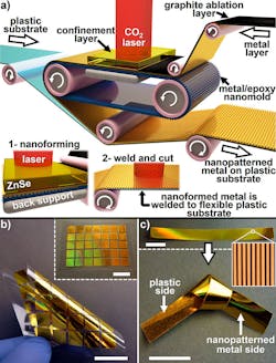
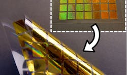
1. The overall R2RLIS implementation: (a) schematic diagram of the pilot line for the roll-to-roll nanoforming of metals; (b) a 5 × 7 tile array of 1-cm2 nanoformed gold domains welded to a flexible PET substrate; (c) nanopatterned gold/PET composite with enough flexibility and interfacial adhesion to withstand bending and being tied into a knot; (inset) a high-resolution AFM image of the ultrasmooth gold nanogratings (350-nm line width). All scale bars are 2 cm. (Source: Purdue University)
The team’s fabrication method uses a rolling stamp similar to the ones used to print newspapers at high speed (Fig. 1). By applying high-energy laser pulses to the material to initiate a high strain rate—a technique called roll-to-roll laser-induced superplasticity (R2RLIS)—the shock wave that the laser induces results in a brief period of "superelastic" behavior in the target.
These shocks, in turn, enable the metal to flow into the nanoscale features of the rolling stamp, and thus gets around the formability limit. By fine-tuning the laser power during the R2RLIS process, it’s possible to control of the aspect ratio (depth/width) as well as the mechanical and optical properties of the fabricated nanostructures. The Purdue team successfully fabricated mechanically strengthened plasmonic nanostructures with aspect ratios as high as five that exhibit high oxidation resistance and strong optical field enhancements.
The technique is applicable to materials in addition to metals. For example, polydimethylsiloxane (called PDMS or dimethicone) is a polymer widely used for the fabrication and prototyping of microfluidic chips. It’s used in to create elastomeric nanostamps that are then used to replicate nanoscale features in a variety of low-cost “soft lithographic” processes, enabling sub-100-nm resolution patterning over curved surfaces and large areas.
However, the fairly low Young’s modulus (the ratio of applied tensile stress to resultant tensile strain) of these stamps makes it difficult to replicate patterns with higher resolution as well as those with high aspect ratio (greater than two). That’s due to the self-adhesion of the stamp features caused by electrostatic attraction, mechanical stress, or capillary forces.
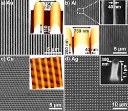
2. Scanning electron microscopy and AFM show the ultrasmooth, 3D nanostructures fabricated by R2RLIS: (a) gold nanograting with a 350 nm line width and a 110 nm height; (b) nano V-grooves with an aspect ratio of 5 (200-nm depth, 40-nm width) fabricated on aluminum; (c) nanoscale fishnet fabricated on a Cu film; (d) array of silver nanopillars, 350-nm diameter/1.1-μm height. (Source: Purdue University)
As discussed in their detailed American Chemical Society Nano Letters paper “Roll-to-Roll Nanoforming of Metals Using Laser-Induced Superplasticity,” the team fabricated different nanogratings (representing various line widths and spacings) in gold and other materials with various aspect ratios using a single titanium/epoxy nanomold with 350 nm width and 220 nm depth (Fig. 2). Gold is used due to its low ohmic loss at optical frequencies and its high oxidation resistance.
By applying different laser-power densities during the nanoforming process, they created 350-nm-wide nanogratings with heights of 50, 75, 100, 120, 136, 169, and 220 nm. Their conclusion is that the R2RLIS techniques can enable the rapid and inexpensive fabrication of ultrasmooth metallic nanostructures suitable for electronics, electro-optics, and optical components over large areas using conventional CO2 laser engravers.

About the Author

Bill Schweber
Contributing Editor
Bill Schweber is an electronics engineer who has written three textbooks on electronic communications systems, as well as hundreds of technical articles, opinion columns, and product features. In past roles, he worked as a technical website manager for multiple topic-specific sites for EE Times, as well as both the Executive Editor and Analog Editor at EDN.
At Analog Devices Inc., Bill was in marketing communications (public relations). As a result, he has been on both sides of the technical PR function, presenting company products, stories, and messages to the media and also as the recipient of these.
Prior to the MarCom role at Analog, Bill was associate editor of their respected technical journal and worked in their product marketing and applications engineering groups. Before those roles, he was at Instron Corp., doing hands-on analog- and power-circuit design and systems integration for materials-testing machine controls.
Bill has an MSEE (Univ. of Mass) and BSEE (Columbia Univ.), is a Registered Professional Engineer, and holds an Advanced Class amateur radio license. He has also planned, written, and presented online courses on a variety of engineering topics, including MOSFET basics, ADC selection, and driving LEDs.
Comment About the Article
To join the conversation, and become an exclusive member of Electronic Design, create an account today!

Leaders relevant to this article: