PCI Express Clock Generators, Buffers Prepare for Next Generation
Download this article in PDF format.
Bracing for the coming 5th generation (Gen5) of PCI Express (PCIe), high-speed serial bus designers are revisiting clocking generators and distribution buffers. This article reviews these fundamental elements in light of the transition from Gen4 to Gen5 PCIe architectures.
Sponsored Resources:
- Comparing and Contrasting PCIe and Ethernet Clock Jitter Specifications
- PCIe Gen 4 Clock Generators, 9FGV100x Family
- PCI Express® Timing Solutions
Clock Generators
PCIe has been around since 2004. It’s a high-speed serial computer expansion bus specification that replaces older PCI and PCI-X standards. PCIe currently supports the Generation 4 specification. In June 2017, the PCI-SIG preliminarily announced the PCI Express 5.0 specification, which is expected to be standardized in 2019.
Regardless of the generation of the PCIe bus, the clock remains the most basic hardware component. The clock generator produces the timing signal that controls the data rate of the bus. Traditionally, a clock buffer is used to control the rise and fall time of the clock edges. Maintaining the cleanest clock rise and fall time is made difficult by the presence of jitter, which causes the clock edge to degrade from it ideal location and shape. Clock jitter is typically induced by the generator circuitry, thermal noise, power-supply variations, and interference coupled from nearby circuits.
As a high-speed serial interface, the PCIe data channel runs at speeds up to 8 Gb/s, increasing to 16 Gb/s with PCIe Gen4 devices. These devices have been used in data centers and networks including servers, SSDs, NICs, FPGA- and GPU-based accelerator cards, and Ethernet and optical modules.
As the data speeds increase with each generation of PCIe bus, so does the potential for jitter. Yet the actual jitter specification for the clock is constantly lowered to meet speed and timing issues. For reference, the PCIe Gen4 jitter limit is 500 femtoseconds (fs) rms, whereas the Gen3 limit was 1 picosecond (ps) rms. The proposed jitter budget for the reference clock in a PCIe Gen5 system is 250 fs max.
Thus, the clock generator is the most crucial element in maintaining the proper PCIe system performance and reliability.
Clock Buffers
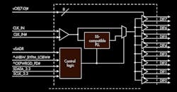
Only a certain number of clocks are allowed in a single device. Such restrictions are the results of a limitation on the number of pin-counts per devices. Also, board wiring routing constraints may limit the number of clocks that are located in a specific area. For these reasons, PCIe clock distribution devices are used in all but the smallest of PCIe bus systems. The distribution devices act as buffers (Fig. 1).
1. Clock-distribution devices are used to condition, manipulate, and distribute clock signals within a system, with or without the use of a phased-locked loop (PLL). (Courtesy of IDT)
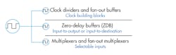
Fan-out buffers allow a single clock to be routed to a section needing multiple clocking inputs, where the buffer then fans (or distributes) out the clock locally. Sometimes, the designer only has a single PCIe clock coming from a connector and needs multiple copies. Again, fan-out buffers address this shortcoming.
Clock trees are built using fan-out buffers to provide signal buffering and low-jitter copies of the original clock signal. The clock fan-out from a single input reduces loading on the preceding driver and provides an efficient clock-distribution network (Fig. 2).
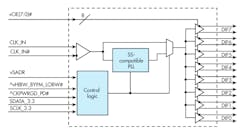
2. This PCIe clock tree with fan-out buffers is from a single clock input source. (Courtesy of IDT)
Finally, zero-delay buffers (ZDBs) provide a synchronous copy (no propagation delay) of the input clock at the outputs. Creating a synchronized copy is accomplished by using phase-locked-loop (PLL)-based devices to regenerate the input clock signal, from which a new fan-out is formed that can drive multiple loads. ZDBs are often used by applications requiring synchronized clocking for FPGAs, CPUs, logic, and synchronous memory.
Clocking Example
Imagine that you have a fairly straightforward design—known as “common clocking”—where all of the clocks come from one source such as a PLL. The clock signal may need to be spread to other parts of the board or not, but it’s unlikely that all of the signals will come from one device. This means that fan-out buffers will be needed to distribute extra copies of the PCI Express clock.
If the design isn’t using spread-spectrum clocking (SSC), then the fan-out to the buffers could be a ZDB with a PLL inside or simply a fan-out buffer (Fig. 3). Either implementation will satisfy the common clock requirement of the PCIe standard. SSC is a technique where the clock frequency is modulated slightly to lower the peak energy generated by a clock to help reduce total system electromagnetic interference (EMI).
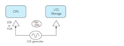
3. This PCIe common clock architecture uses no spread spectrum copies (SSC), but rather zero-delay buffers (ZDBs) or fan-out buffers (FOBs). (Courtesy of IDT)
IDT’s family of PhiClock programmable clock generators represents a good example of timing devices. These generators can be configured via select hardware pins or software. Part of the family provides several non-spread-spectrum copies of a single output frequency, copies of the crystal reference input, and fractional frequency copies of the original clock signal.
In addition, IDT PCIe clock generators support 1.5-, 1.8-, or 3.3-V versions, allowing the designer to power the clocks from the same power supply as an FPGA or system on chip (SoC).
On the buffer side, IDT’s 9Z enhanced PCIe buffer family offers buffers with and without a PLL inside. The PLL creates a ZDB that eliminates propagation delay through the device, which reduces transport delay. If the PLL is bypassed, the unit converts into a pure fan-out buffer (no PLL). If the design uses spread spectrum, then a pure fan-out buffer is needed most of the time.
Taken together, both the PhiClock clock generator and 9Z buffers offer performance upgrades by providing a 50% margin to the PCIe Gen4 clock jitter limit of 0.5 ps rms. Initial IDT testing shows both families satisfy upcoming Gen5 PCIe requirements. For more information, please visit www.idt.com/pcietiming.
Summary
Clock generators and buffers will continue to play a critical role in PCIe specifications and performance. IDT has Gen4 PCIe clock-tree devices that meet the soon-to-be-released Gen5 standard.
Sponsored Resources:
About the Author
John Blyler
John Blyler has more than 18 years of technical experience in systems engineering and program management. His systems engineering (hardware and software) background encompasses industrial (GenRad Corp, Wacker Siltronics, Westinghouse, Grumman and Rockwell Intern.), government R&D (DoD-China Lake) and university (Idaho State Univ, Portland State Univ, and Oregon State Univ) environments. John is currently the senior technology editor for Penton Media’s Wireless Systems Design (WSD) magazine. He is also the executive editor for the WSD Update e-Newsletter.
Mr. Blyler has co-authored an IEEE Press (1998) book on computer systems engineering entitled: ""What's Size Got To Do With It: Understanding Computer Systems."" Until just recently, he wrote a regular column for the IEEE I&M magazine. John continues to develop and teach web-based, graduate-level systems engineering courses on a part-time basis for Portland State University.
John holds a BS in Engineering Physics from Oregon State University (1982) and an MS in Electronic Engineering from California State University, Northridge (1991).
Comment About the Article
To join the conversation, and become an exclusive member of Electronic Design, create an account today!

Leaders relevant to this article: