Wood-Based 3D-Printed Sensors Include Wireless Access

Using wood—or to be more precise, cellulose derived from wood—is a hot R&D material, perhaps due to its biocompatibility and sustainability potential. A joint research team from Simon Fraser University (BC, Canada) (Fig. 1), and the Applied Wood Materials Laboratory at the Swiss Federal Laboratories for Materials Science and Technology (EMPA, Zurich) has developed 3D-sensor systems printed on cellulose that are disposable, ion-selective, and can be interrogated wirelessly. These sensors offer what the researchers maintain are a unique combination of form factor, high sensitivity, and flexibility.
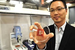
1. Simon Fraser University Mechatronic Systems Engineering professor Woo Soo Kim holds one of the sensors developed by the multi-institute team (Source: Simon Fraser University)
The goal is to replace the plastic of common printed circuit boards (PCBs) with eco-friendly and disposable chemical sensors. “If we are able to change the plastics in PCB to cellulose composite materials,” noted project leader Professor Woo Soo Kim (SFU professor at FSU’s School of Mechatronic Systems Engineering), then “recycling of metal components on the board could be collected in a much easier way.”
To achieve this, they used a printable conductive ink that’s designed and optimized for cellulose nanofibers (CNFs) by adding silver nanowires (AgNWs). For better resolution of the printing, they used a polyimide film that has high surface hydrophobicity as a substrate. They were able to create 3D-printed sensor circuits that included inductor–capacitor (LC) circuits along with ion-selective membrane electrodes (Figs. 2 and 3). These electrodes can be tailored to selectively detect quantitative ion concentrations.
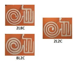
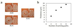
2. These three 3D-printed inductor-capacitor (LC) circuit samples have different thicknesses with different printing paths; for example, 2L8C contains a double-layered inductor and 8-layered capacitor. (Source: Simon Fraser University)
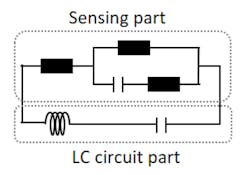
3. The equivalent circuit of the sensor system consists of an ion selective membrane electrode (ISME) for the sensing part and an inductor-capacitor (LC) circuit. (Source: Simon Fraser University)
The change of ion concentrations is reported wireless by measuring the magnitude of S11 (the reflective coefficient S-parameter, also known as gamma or Γ, the return loss) at the resonant frequency of 2.36 GHz using a vector network analyzer (VNA) and loop antenna (Fig. 4). Among their many tests, Figure 5 shows the change in magnitude of S11 for the ion-selective membrane electrode (ISME) with four different concentrations of NH4Cl solution.
4. A VNA and loop antenna are used to “read” the sensor-produced signal via variations in S-parameter S11. (Source: Simon Fraser University)
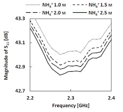
5. The change in magnitude of S11 in ISME (with a NH4+ membrane) shows the frequency change, with four different concentrations of NH4Cl solution. (Source: Simon Fraser University)
Full details are of the wireless, cellulose-based sensor are published online in Advanced Electronic Materials in their paper “Electrochemical Sensors: 3D Printed Disposable Wireless Ion Sensors with Biocompatible Cellulose Composites,” along with Supporting Information. The project is truly a global collaboration, as the printing process used is itself the result of collaboration between the same Simon Fraser University team and another group at DGIST, the Daegu Gyeongbuk Institute of Science and Technology in Korea. Details of that project were previously described in a paper also at Advanced Electronic Materials, “Impact Print‐Type Hot Embossing Process Technology” and summarized in a news report at the phys.org section of the Science X Network, “New breakthrough in hot embossing technology.”

About the Author

Bill Schweber
Contributing Editor
Bill Schweber is an electronics engineer who has written three textbooks on electronic communications systems, as well as hundreds of technical articles, opinion columns, and product features. In past roles, he worked as a technical website manager for multiple topic-specific sites for EE Times, as well as both the Executive Editor and Analog Editor at EDN.
At Analog Devices Inc., Bill was in marketing communications (public relations). As a result, he has been on both sides of the technical PR function, presenting company products, stories, and messages to the media and also as the recipient of these.
Prior to the MarCom role at Analog, Bill was associate editor of their respected technical journal and worked in their product marketing and applications engineering groups. Before those roles, he was at Instron Corp., doing hands-on analog- and power-circuit design and systems integration for materials-testing machine controls.
Bill has an MSEE (Univ. of Mass) and BSEE (Columbia Univ.), is a Registered Professional Engineer, and holds an Advanced Class amateur radio license. He has also planned, written, and presented online courses on a variety of engineering topics, including MOSFET basics, ADC selection, and driving LEDs.
Comment About the Article
To join the conversation, and become an exclusive member of Electronic Design, create an account today!

Leaders relevant to this article: