Why are Specification and Characterizations for Op Amps and FDAs Different and Confusing?

This article is part of the TechXchange: Exploring Op Amps.
Members can download this article in PDF format.
What you'll learn:
- Who is involved with simulating op-amp design and developing their datasheets?
- Clarifications on sometimes obtuse amplifier specifications.
- Pitfalls to avoid when interpreting ac specs.
- What to watch for in vendor-supplied simulation models.
It can be a maddening (and time-consuming) task to compare data across vendors to get a real comparison between possible solutions. Between “marketesse” and just plain deception and/or errors, how can you see through these and normalize critical specs across vendors to get real comparisons.
Having contributed to the development and product launch of over 150 high-speed amplifiers from 1985 forward, the level of detail and tradeoffs going into product datasheets and simulation models probably exceeds the wildest imaginings of the end-system designers. Here you will learn some of the hidden background for (and often confusing) specifications along with what to look out for in characterization curves and vendor simulation models.
First, who does this work and what do they bring to the task?
IC design engineer
The designer, working with the latest process design kit (PDK) takes the marketers end-product targets and iterates over many months to get close. Usually, these targets take the form of more and more performance at lower and lower supply current.
Occasionally, a new topology will come along that fills an important niche, such as the fully differential amplifier (FDA) and current feedback amplifier (CFA). Once the nominal transistor-level topology is set, he/she will start running statistical process case and over-temp simulations to extract out corner cases for the proposed end limits on key specs. PDKs have evolved to be remarkably good; only some of that gets into the datasheet and customer simulation models.
Marketing engineer
Looking at the extant solution universe, the marketing engineer tries to carve out unique and valuable new product targets. Through the course of design and introduction, he/she trades off “don’t care” versus “must care” specs with the designer to hopefully emerge with a meaningful new solution for the analog design community.
ATE engineer
This key team member is tasked with layering over a set of probe and/or finished product tests to ensure nothing ships that’s defective. In the early days of high-speed amplifiers, 100% ac testing was done at Comlinear Corp on the industry’s first current feedback op amps using an HP3577 network analyzer. Over time, it became clear that a full suite of stressful dc tests shipped good ac parts and that production expense was eliminated.
With a few exceptions, all current precision and higher-speed amplifiers receive only a dc test at probe and/or final test at some nominal temperature (with some span on that), imputing ac performance within the designer worst-case simulation results.
The ATE engineer is incentivized to deliver tests and limits with 100% yield. The marketing engineer must resist this—say, on input offset voltage, a ±3.5-sigma test limit is probably adequate (implying no more than 0.04% yield loss). Expanding single-lot ATE data to final datasheet limits is largely internal culture, designer simulation tools, and judgement calls among the development team members and any QA mandates that might be imposed.
Applications engineer
Directed by the marketing engineer, and with an assist from design, the application engineer is tasked with taking the characterization curves and working with the modeling team to develop and test the public simulation model. This is where the rubber meets the road in what the customer sees as a product support package. He/she will also add suitable application text and examples to the final datasheet to illustrate the fabulous new capability for a device that probably cost well over $1M to develop.
Personnel and Datasheet “Churn”
One of the difficulties with consistent and accurate material is the relative turnover in these positions. Often, the designer and ATE engineer are 20-plus-year folks. There’s quite a bit of churn in the marketing and applications roles where the latter might be just out of school. Hence, a very tenuous thread links today’s datasheets to those done even 10 years ago (and nearly none to those done 20 years ago).
At a more basic level, no NIST reference document exists on how the different specs and characterization curves “must” be done. In fact, on some of the critical specs, there’s been an ongoing evolution of better methods.
For instance, when I first started doing distortion plots (circa 1987), about −90 dBc was the measurement limit imposed by spectrum analyzers. Today, bench techniques reach down near −150 dBc (if you want to spend enough effort on it, very non-trivial—operating above audio precision measurement frequency range).
Clarifications on Occasionally Murky DC Specs
Most of the op-amp and FDA dc specifications are pretty clear. Some, but not all, of the dc specifications become the final test lines. A few can cause confusion at times, particularly those with a zero mean as well as the output current specification.
Input offset voltage
The input offset voltage (and current for bipolar inputs) will usually have a distribution centered on zero. Modern devices trim this to a zero mean at either wafer probe or packaged eTrim. So what do you specify for a typical, because “0” doesn’t really give you much information?
The informal practice across the industry is to report the ±1-sigma number as the typical specification to avoid customer surprises when devices with a zero mean don’t test at zero for typical devices. Specifications for a maximum input offset voltage (and current where needed) are extremely inconsistent. Essentially those are a combination of a plus/minus shift of the mean off of zero plus/minus some number of standard deviations.
My practice was to impose a ±3.5-sigma range (THS4551) to accept approximately 0.04% yield loss. Other devices and product groups allow for much wider limits (OPA837, THP210, ADA4805, etc). Some of this is related to test repeatability, where there’s also an error band in test over different physical testers. While this might pass more units, you do wonder if devices way out on the distribution tails (some allow for >8 sigma) might be shipping “defective” units.
These same issues apply to the specified input-offset-voltage temperature drift, where it’s extremely rare to see this as a 100% tested specification (the JFET input OPA656 is one of the very few). Maximum offset drift numbers are sometimes provided without ATE screens (OPA2683A, ADA4895), while many more devices have no maximum drift spec(s).
The guaranteed maximum drift numbers are from extensive bench characterization of packaged units that are (hopefully?) at the extreme allowed limits of the tested room-temp input offset voltage (and current where appropriate). Drift magnitude is often linearly related to initial offset, so testing units at the allowed limit should expose the worst-case drift specs.
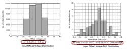
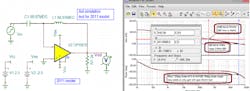
Figure 1 shows a recent example where the tested Vos limits are ±95 μV (or ±10 sigma), imputing a drift limit of ±1.2 μV/°C or ±4 sigma. The actual Vos histogram data in Figure 1 is much tighter than the ATE limit in the specification table. Apparently, the ATE engineer got this through while the marketer was out traveling.
Output current
Probably the most slippery dc specification on any op-amp or FDA datasheet is the output current. Marketers want the biggest number possible. Designers struggle with that as large output devices bring an increased capacitance, which adds open-loop phase shift that impairs achievable bandwidth on ever-declining supply current budgets. ATE engineers are all over the map in how this might be tested.
Physically, the output-current demand will get involved with the available “linear” output-voltage swing available. Every device (even rail-to-rail outputs) will see an increase in required headroom to the supplies for linear operation due to rising load-current demand. Keep in mind that not only the actual load, but also the feedback network, is part of that load. In non-inverting configurations, that’s the sum of the feedback and gain resistors, while in inverting configurations (and for FDAs), it’s just the feedback resistor appearing in parallel with the actual load.
First, it’s important to recognize that any “short circuit” current specification is usually a self-limited (base or gate drive) typical specification. Traditionally, it needs to be there, but it doesn’t really give you much information. Only when there is a min. or max. specification is there an “active” current limit in the output stage design (THS3491), with some exceptions (OPA2683A).
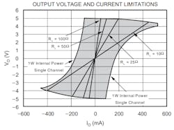
Over time, several different efforts at a “linear” output-current specification have been attempted. During the PLC line-driver developments (where the line can push current back into an amplifier output), a foour-quadrant envelope of limits was shown—like that in Figure 2 taken from the OPA2674 datasheet (on ±6-V supplies). Only the quadrants with the load lines describe normal operation here.
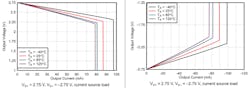
More typically, a bipolar “claw” curve has evolved to describe the loss of output headroom, as more sourcing or sinking current is required. Here, the two polarities are separated into two plots, but the increase in required headroom with output source/sink current is clearly shown in Figure 3.
These output limits are hard limits (usually from simulation). However in final ATE, a more common test is a minimum Aol test at some conservatively guardbanded (25°C) test point. It exercises most of the available output current (from worst-case designer simulations at 25°C) at the maximum swing to rail available at that current draw, as shown in Figure 4 for the OPA837.

Here, the final ATE test lines are clearly designated by the “A” test level, and the test conditions to produce these stated output currents are shown (using ±2.5-V supplies in this case). This type of ATE screen is intended to ensure that no “weak” output stage devices are getting into inventory.
These issues apply to all op amps and FDAs. It is, however, often not clearly shown in the customer support material and almost never accurately modeled in the vendor simulation models.
Common Hazards in Interpreting Op-Amp and FDA AC Specs
If the dc specifications have some typical traps, the ac specifications are often much worse. Again, none of these are tested on an outgoing basis and the typical—and much more rarely guaranteed—ac specifications (e.g., OPA2677) come completely from simulation. Usually, a single (hopefully typical) lot of early material is characterized one time at product release.
Vendor models are normally bounced against typical designer simulation with some first-lot material validation. A few very typical performance parameters are prone to error and/or confusion.
Input spot noise
The input spot noise voltage must be in every datasheet. Physically, these always have a 1/f corner that varies considerably more than the higher-frequency “flatband” number (except for chopper-input VFAs, which have a flat noise spectrum down to dc but then add noise spurs at the higher chopper frequency).
A very old convention for relatively slow (often precision) amplifiers is to report an input spot noise at 1 kHz. This apparently came out of the audio world and the 1-kHz number may be above, or below, the 1/f corner. It’s much more descriptive to specify a typical flatband number (most higher speed amplifiers do this) above the 1/f frequency and then a typical 1/f corner.
However, many VFAs quote a single noise number and only after some digging can you discern if that’s the 1-kHz number. You must then consult the swept-frequency input spot noise plot to decide what that means.
Gain bandwidth product
The second most confusing ac specification has become the typical gain bandwidth product (GBP) for VFA op amps and FDAs. Classic theory describes this as the 1-pole projection to 0-dB crossover for the devices’ Aol curve. Modern devices have higher-frequency open-loop poles (and sometimes pole/zero pairs, LT6363) in the Aol response that convolutes this quite a bit.
Since the new product characterization folks are a revolving door of new grads, many datasheets erroneously report the GBP as the Aol = 0 dB frequency.1 That’s never very close for decompensated devices and often even a bit off for unity-gain stable devices. This confuses new grads quite a bit since the closed-loop small-signal BW (SSBW) never really was accurately described by the GBP idea even for unity-gain stable VFAs.1 Lower phase margins at loop-gain (LG) crossover always extend the closed-loop SSBW far beyond the GBP model (below 65-deg. phase margin, which is approximately a 1.6X extension).
Sometimes, those new grads try to force a fit to the simple GBP model by modifying what they report. It’s always best to confirm the single-pole GBP in simulation for design work (go to the 40-dB Aol gain frequency and multiply that by 100X to get the single pole GBP, Figure 6 shows a simulation setup, see below). Oftentimes, that’s far different than what shows up in the datasheet, and hopefully the modeling effort worked closely with the designer to emulate the new devices’ typical Aol gain and phase-match the designer PDK simulations.
Slew rate
Slew rate has long been a difficult specification and fraught with error. Early ±15-V op amps showed a very distinctive, limited dv/dt on a large output transition. Sometimes those are different for rising and falling, where reporting the faster rate in the specification table is not uncommon. With few exceptions, a signal that rises with a certain maximum rate must also fall at a similar rate. Check the plots to see if this bit of chicanery is at play (Figure 39 in the OPA192 datasheet).
In most applications, the available slew rate is like a hard output transition rate that should be avoided, if possible, in application. By definition, the feedback loop has opened up if the output is slew limiting where that recovery time to a closed-loop final condition is rarely specified—and if so, only for limited number of external operating conditions.
The best way to explore edge transition rates is to plot the measured or simulated point by point dv/dt on the edges.2 This will clearly show when an edge has hit a slew limit (flat dv/dt) and more detail is going into and out of slew limiting.
Harmonic distortion
One of the more difficult characterization requirements in any new op-amp or FDA development is a range of typical harmonic-distortion plots. These have evolved over the years to show performance to ≤145 dBc on occasion. The main reporting difficulty is all of the different conditions that influence the measured values, including:
- Supply voltages
- Gain (more precisely, the loop gain over the testing frequency span)
- Output loading (and this includes the required feedback network)
- Output voltage swing
- Frequency of the test fundamental (or two of these for two-tone intermodulation testing)
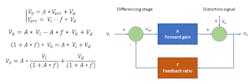
This myriad of test conditions does make it relatively difficult to compare data across different possible solutions. It’s important to always keep in mind some fundamental harmonic-distortion facts. Essentially, the output closed-loop distortion terms are the open-loop distortion terms in the output stage corrected by the LG at the fundamental frequency of testing. The LG is Af in Figure 5.
The easiest way to show a better HD number in characterization is to test with a lighter resistive load. Be careful comparing devices on their stated loading under test.
Hidden Traps in Vendor-Supplied Simulation Models
As a new op amp and/or FDA approaches public release, the modeling effort gets underway. Over time, several approaches have dominated:
- Simplified full transistor-level models: These can be very good if the embedded transistor models capture enough of the available parameters (Comlinear models, full netlists are in the TINA libraries showing detailed transistor models).3 Some transistor-based models use such a simplified core transistor model that they’re nearly useless.
- Boyle model: This is more of a behavioral model that does okay on basic things, but often isn’t very accurate.4
- Custom block diagram types of models that can capture quite a lot of the device characteristics:5 In this case, the internals are often company confidential and sometimes those models are encrypted.
How this is organized inside a company makes a huge difference in the effectiveness of these models. Some groups have each project’s individual application engineer and/or designer do these (which leads to lots of modeling variations). Some have a dedicated modeling group that usually leads to throughput bottlenecks. Others have a designated applications specialist in each development group that becomes the resident expert. This will yield better and better models with some consistency, until they move on to another job.
One theme here is that the op-amp and FDA models have been getting regular updates from some of the vendors. Designers should certainly try to verify that they’re using the most recent update, as earlier (more error-prone) models are still available from some legacy sources.
Importantly, the vendor models must assign some typical dc value specifications where their “range” is never captured. Therefore, dc parameters are just enough—they don’t span the full range of the datasheet specification limits. Far more effort is put into the ac performance characteristics, but again, only typical. To get a good prediction of small-signal ac performance over a wide range of external application circuits, the model must have very good:
- Open-loop gain and phase modeling.
- Open-loop output impedance modeling (this has become relatively involved with RRout devices).
- Accurate input impedance modeling. This is usually mainly input capacitance, but for CFA devices a good inverting-input impedance model is necessary (usually just a low R value; however, for instance, the THS3217 OPS model includes a series RL into the inverting input and parasitic C to ground on that device pin).
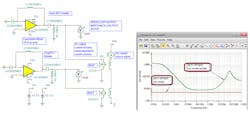
An op amp’s open-loop gain or phase is really the core value proposition for the ac aspect of the device. There are numerous approaches to extracting this from the vendor model. Figure 6 shows one simple approach.
Typically, these are done with split bipolar supplies with the V+ input grounded and the test signal injected into the inverting input. It’s critical to load the amplifier with the stated resistive (and/or capacitive) loads noted in the datasheet.
This approach applies a simulation trick to close the loop at dc at unity gain using a ludicrously high feedback L value, and then injects the small-signal ac test input through an equally high input capacitor. These elements set up a midscale dc operating point and then disappear on the first ac frequency step. Since the input is into the inverting input, the output meter here is rotated 180 deg. to report Aol, where its phase starts out at 0 deg. and proceeds toward −180 deg.
This model shows quite a bit more GBP than the specified typical of 31 MHz. The 0-dB crossover is less than the predicted single-pole GBP due to the higher-frequency Aol poles indicated by the phase shift moving down −90 deg. from the single pole. This OPA835 model is now updated to a 2017 revision, where this simulation shows a correct 31-MHz GBP projecting from a 40-dB Aol point.
One of the modeling oversights receiving much attention in recent years is the open-loop output impedance. Early bipolar op amps and FDAs offered a very power-efficient Class AB output stage that delivered lots of current with a low dc open-loop output resistance going inductive at higher frequencies.
Those required considerable headroom for the supplies, where more recent devices have gone to RRout structures. The output stages show a considerably more involved open-loop output impedance6 that was completely missed in much of the original modeling. They’re getting updated over time as shown in the OPA835 Zol simulation of Figure 7, going from the 2011 to 2017 model updates. The high-frequency resonance in the RRout Zol can sometimes lead to closed-loop peaking or oscillations with relatively simple external conditions.7
The last key issue for accurate ac modeling involves the input impedances. For VFA op amps, these are usually just the common-mode and differential-mode input capacitances. Usually, these relatively low value elements will not interact with lower-speed (<10 MHz) device applications, but they become critically important for higher-speed op amps and FDAs.
Once again, some of the legacy models have these in the model incorrectly, where that’s being repaired over time. At minimum, when using a higher-speed device in simulation, confirm that the model values match the datasheet values (from designer sims) using the approaches detailed in Reference 8.
As you endeavor to select and apply modern op-amp and FDA devices, keep in mind some of these inconsistencies across vendors and modeling pitfalls that pervade the industry. Working through these can be difficult, but when armed with what to look out for, supplier application teams can be a great help.
Read more articles in the TechXchange: Exploring Op Amps.
References
1. “Why is amplifier GBP so Confusing,” Michael Steffes, Planet Analog, 9/23/2019.
2. “What is op amp slew rate in a slew-enhanced world? ,” Michael Steffes, EDN, 1/8/2017.
3. “Simulation Spice Models for Comlinear’s Op Amps ,” TI application note, OA-18, May 2000.
4. “Analog Circuit Simulation ,” Analog Devices Tutorial, MT-099.
5. “Building an Accurate SPICE Model,” Don LaFontaine, Renesas application note AN1556, 4/19/2010.
6. “Designing with a complete simulation test bench for op amps, Part 1: Output Impedance,” Ian Williams, EDN, 3/16/2018.
7. “Stability Issues for High Speed Amplifiers,” Michael Steffes, Planet Analog, 2/3/2019.
8. “Input Impedance Extraction and Application for High Speed Amplifiers,” Michael Steffes, Planet Analog, 6/7/2019.
About the Author

Michael Steffes
Analog Signal Path Consultant
Starting as an IC design engineer at the original current feedback amplifier company (Comlinear), I progressed through 35 years of high speed amplifier development projects. Through these years I contributed to the definition, development, and product launch (datasheets and simulation models) of over 150 high speed amplifiers. Generating the related technical collateral also produced over 150 contributed articles and application notes..
Comment About the Article
To join the conversation, and become an exclusive member of Electronic Design, create an account today!

Leaders relevant to this article: