MOSFET H-bridge Reduces Footprint by 50%
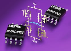
A pair of MOSFET H-bridges from Diodes Inc. simplifies motor driving and inductive wireless charging circuits by cutting component count and reducing PCB footprint by 50%. The 40 V-rated H-bridge, the DMHC4035LSD, is targeted at meeting the requirements of automotive motor driving applications, whereas the 30 V-rated H bridge, the DMHC3025LSD, is suitable for 12V single-phase fan applications.
By packaging dual N-channel and dual P-channel MOSFETs to make a full H-bridge in just a single 5mm x 6mm SO-8 footprint, the DMHC3025LSD and DMHC4035LSD replace the equivalent four SOT23 or two SO-8 packages for a wide range of space-constrained automotive and industrial applications, including: low-power DC brushless motor driving, fan control and similar requirements for driving inductive loads.
The H-bridges' space-saving advantage is complemented by the lowRDS(ON) performance of the MOSFETs: typically 45 mW at 10V VGS and 65 mW at -10 V VGS, respectively, for the 40 V N-channel and P-channel devices. The minimal conduction losses resulting from the low on resistance mean the H-bridges are able to tolerate higher continuous current under motor stall conditions. Under +70 ºC high ambient operating temperature, the 30 and 40 V H-bridges can support continuous currents of 3 A and 2 A, respectively, thereby accommodating worst-case motor stall currents.
The DMHC3025LSD and DMHC4035LSD H-bridges from Diodes Incorporated are priced at $0.40USD each in 10k quantities.

