CXL: Coherency, Memory, and I/O Semantics on PCIe Infrastructure

Members can download this article in PDF format.
What you’ll learn:
- Gain insight into the CXL specification.
- Learn how CXL supports dynamic multiplexing between a rich set of protocols that includes I/O (CLX.io, based on PCIe), caching (CXL.cache), and memory (CXL.mem) semantics.
- Understand how CXL maintains a unified, coherent memory space between the CPU and any memory on the attached CXL device.
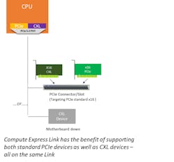
The Compute Express Link (CXL) is an open industry-standard interconnect offering coherency and memory semantics using high-bandwidth and low-latency connectivity between host processor and devices such as accelerators, memory buffers, and smart I/O devices. CXL is based on the PCI Express (PCIe) 5.0 physical-layer infrastructure with plug-and-play interoperability between PCIe and CXL devices on a PCIe slot (Fig. 1).
CXL is designed to address the growing needs of high-performance computational workloads by supporting heterogeneous processing and memory systems with applications in artificial intelligence (AI), machine learning (ML), communication systems, and high-performance computing (HPC). Coherency and memory semantics in a heterogeneous environment are increasingly important as processing data in such emerging applications requires a diverse mix of scalar, vector, matrix, and spatial architectures deployed in CPUs, GPUs, FPGAs, SmartNICs, and other accelerators.
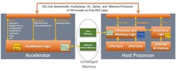
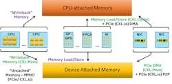
CXL achieves these objectives by supporting dynamic multiplexing between a rich set of protocols that includes I/O (CXL.io, which is based on PCIe), caching (CXL.cache), and memory (CXL.memory) semantics (Fig. 2). It maintains a unified, coherent memory space between the CPU (host processor) and any memory on the attached CXL device. Thus, both the CPU and CXL device can share resources for higher performance and reduced software stack complexity.
Moreover, since the CPU is primarily responsible for coherency management, it can reduce device cost and complexity as well as overhead traditionally associated with coherency management across an I/O link. In this article, we delve into some details of CXL 1.0 and CXL 1.1 specification and usage models. Additional details can be found in the references (see References at the end of the article).
Caching and Memory Semantics
PCIe devices transfer data and flag across the PCIe Link(s) using the load-store I/O protocol while enforcing the producer-consumer ordering model for data consistency. This works well for bulk transfers. However, where the data access has either spatial or temporal locality (i.e., the same data is repeatedly accessed and/or where accesses are to sequentially increasing addresses), or in cases where the data access is sparse (i.e., a small percentage of the data is really accessed), caching semantics helps tremendously. That’s due to the efficiency of moving only the needed data and moving it only once.
The device can cache only the data that it needs. Caches provide low-latency (~10-ns access latency) and high-bandwidth (~150 GB/s) accesses if the location is cached by the device. It’s much more efficient than the ~500-ns access latency and ~50-GB/s bandwidth in accessing a memory location across a non-cached interconnect. This is useful for CXL accelerators represented as Type-1 and Type-2 CXL devices (Fig. 3).
Caching also enables efficient implementation of complex semantics such as advanced atomics and advanced telemetry used by devices like SmartNICs. Once a device caches a memory location, it can implement any advanced semantics since it’s guaranteed to be performed atomically within the 64-byte cache line boundary.
Another example is networking devices implementing advanced inter-process communication mechanisms such as partitioned global address space (PGAS). Ordering semantics of such mechanisms can be performed efficiently with cache coherency by the device. If the SmartNIC implementing PGAS was a PCIe device, it had to wait for a read request to complete before launching a subsequent write on the PCIe Link since writes in PCIe are in a different flow-control class and can bypass prior reads.
Caching enables the device to prefetch the ownership of the cache line to be written while it requests the read data; it doesn’t have to wait for the write to be flushed to the system memory since completing the write in the local cache ensures architectural global visibility. Thus, the device can pipeline its accesses through coherent accesses and deliver better throughput.
CXL.memory allows a host processor or other CXL devices to access memory attached to a CXL device. CXL.memory transactions are simple memory load and store transactions that run downstream from the host processor, which takes care of all associated coherency flows. Memory accesses are always for a single cache line, which is 64 bytes. Therefore, a Type-2 device can allow the host processor (or other CXL devices) to access its memory coherently without having to copy over the contents of its memory.
The other major usage involves Type-3 devices, which enables the construction of memory buffers that can be used to build additional capacity and bandwidth while remaining open to any type of memory device, including DRAM, RRAM, 3DXP, SSD, etc. This will help people innovate on new memory types while exploring new usage models such as near-memory processing.
Asymmetric Coherency and Memory Protocol for Simplicity
CXL is an asymmetric protocol (Fig. 2, again). It implements the hardware-managed MESI (Modified, Exclusive, Shared, Invalid) protocol for ensuring data consistency for CXL.cache and CXL.memory protocols. The Home agent, residing in the host processor, is responsible for orchestrating cache coherency and resolving conflicts across multiple caching agents (CXL devices, local cores, other CPU sockets, etc.). The device merely has a caching agent and implements a simple set of commands (e.g., requests, snoops, etc.).
There are three message classes, each with its independent flow-control/credit, per direction for CXL.cache: Request (Req), Response (Rsp), and Data. The Data carries the cache line data payload for a transaction to the Req or Rsp type, if it has data. In the device to host direction (D2H), CXL.cache Req includes read requests (e.g., Rd_shared, RdOwn for exclusive access) and write requests. The corresponding host to device (H2D) response indicates the global observability (GO).
The H2D Req is basically different flavors of snoops (e.g., SnpInv, SnpCur) and the response (e.g., RspI, RspSHitSE) indicates the response along with the state of cache line in the device following that response. CXL.cache is unordered within and across message classes with the exception that a snoop must push GO to the same cache line to enforce the MESI protocol, which can occur due to conflicts. Conflicts occur when multiple caches want access to the same cache line at the same time, which is resolved by the host processor.
Figure 4 demonstrates an example of conflict resolution and protocol flows that’s orchestrated by the Home agent in the host processor. It also demonstrates how CXL devices are oblivious to these complex conflict flows and simply respond to snoop requests.
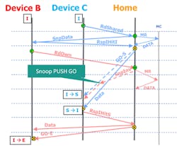
Two CXL devices, B and C, request the same cache line for exclusive and shared ownership, respectively. The Home agent receives C’s request first and provides both the data as well as shared ownership (GO-S). However, a subsequent snoop arising due to B’s access (SnpInv) has been sent to C, while the GO-S is still in flight.
The ordering rules require that the snoop be ordered behind the GO-S since it is to the same cache line. This results in C getting the data S, possibly consuming it, prior to invalidating the line (RspIHitS). Without this ordering, C would have provided a RspI if the SnpInv arrived before the GO-S, and the same cache line would have been in E state in B and S state in C, resulting in a MESI protocol violation.
CXL.memory is a transactional and directional protocol between the master (Home agent in host processor) and subordinate (Memory Controller in CXL device). It includes optional support for metadata to track the directory state. All accesses are for cache line and are made using HPA. Only requests are sent from host to device in two channels: M2SReq (e.g., read request), and M2S RwD (e.g., writes). The device to host side only responds on two channels: S2M NDR (no data response) and S2M DRS (response with data).
Memory in a Type-2 device can be mapped as MMIO (memory-mapped I/O) through CXL.io or as write-back memory through CXL.memory. The former is known as device bias and the latter as host bias. The Type-2 device can move a memory location across these two types. CXL defines an architected flow for flipping a memory location across these two biases that ensures data consistency without having to change the page table.
System Capability Enabled by CXL
CXL builds on the non-coherent load-store semantics of PCIe and provides a unified coherent memory space across processors and devices. Figure 5 demonstrates the additional capability provided by CXL. It enables devices to cache system memory and be able to map their memory to system memory, resulting in memory expansion and more efficient data as well as resulting in an exchange between different computing elements at user level. For accelerators, instead of physically moving all data and flags between devices and CPU, and serializing processing, only the accessed data moves around and stays with the accessing entity for as long as it needs it—no one else contends for it.
Similarly, device memory mapped to the system memory also is managed by the Home agent. Device caches are tracked by the host processor through a snoop filter to ensure that the devices don’t receive unnecessary snoops. CXL enables simpler implementation of the device by leveraging the existing Home agent functionality in the host processor, which tends to be tied to the processor micro-architecture. This has enabled CXL to evolve in a fully backward-compatible manner. It also allows CXL devices to implement CXL.cache and CXL.memory with less complexity while protecting their investments due to the CXL strategy of full backward compatibility as the technology evolves.
All accesses in CXL.cache (and CXL.memory) only have a host physical address (HPA). The device must implement a device translation lookaside buffer (DTLB) and use the PCIe Address Translation Services (ATS) on CXL.io to translate the virtual address to HPA for a CXL.cache request. The ATS completion includes indication of whether the device can use the CXL.cache path for accessing the memory location.
CXL Compliance Test Suite
Compliance testing is one of the important pillars of ensuring interoperability for an open standard while ensuring full backward compatibility during the technology’s evolution. Our approach to compliance testing is novel in that users can perform in-system testing without special hardware or a test vehicle such as an exerciser. We use a set of architected registers to automate in-system testing. Each test defines the assumptions reflected in the setup, a set of steps to run the test, and clearly identified pass or fail criteria.
There are seven areas of testing: Application or Transaction layers, Link Layers, Arb/Mux, Physical Layer, Registers, Reset flows, and RAS (Reliability, Availability, and Serviceability). For example, to test the coherency flows in the CXL.cache Transaction Layer level, we use the concept of false-sharing, where a device and the host processor access a set of addresses set up by the testing software running in the system. The test program checks the data consistency in the system itself which is a part of the test. Each set of accesses in a test can be run a finite number of times or until the test process is manually terminated.
Similarly, to test the producer-consumer ordering model of a CXL.io Application Layer, we have an automated mechanism where the host and/or the device reads a range of memory and writes a different range as specified in the configuration registers. Checking is automated in the test to ensure producer-consumer ordering rules are followed. Tests can run anywhere from one iteration to infinite iterations, to help with debug as well as to provide adequate coverage with something like an overnight run. This compliance approach will help enable very-high-quality components in the CXL ecosystem.
Conclusions
In addition to the accelerator and memory expansion devices in a platform, CXL 2.0 supports new usages such as switching, pooling of resources in a rack, persistence memory flows, and security enhancements while maintaining full backward compatibility. Stay tuned for a deep dive on those topics. We’re on the journey to the next evolution of the specification to comprehend more usage models while delivering improved performance.
The CXL Consortium is committed to developing this open standard in a collaborative manner and welcomes active participation of the broader industry. The journey continues with lots of exciting products and innovations in the horizon.
Acknowledgements: We want to thank Rob Blankenship for his help with this article.
References
1. D. Das Sharma, G. Ward, and K. Bowman, “An Introduction to Compute Express LinkTM (CXL) Technology,” CXL Consortium Webinar, Dec 12, 2019.
2. S. Tavallaei, R. Blankenship, and K. Lender, “Exploring Coherent Memory and Innovative Use Cases,” Webinar, CXL Consortium, Mar 12, 2020.
3. C. Petersen and P. Chauhan, “Memory Challenges and CXL Solutions,” Webinar, CXL Consortium, Aug 6, 2020.
About the Author

Debendra Das Sharma
PCI-SIG Board Member, UCIe Consortium Chair, and Intel Fellow, Intel Corp.
Dr. Debendra Das Sharma is an Intel Fellow and Director of I/O Technology and Standards Group. He is an expert in IO subsystem and interface architecture, delivering Intel-wide critical interconnect technologies in Peripheral Component Interconnect Express (PCIe), coherency, multichip package interconnect, SoC, and rack scale architecture. He has been a lead contributor to multiple generations of PCI Express since its inception, a board member of PCI-SIG, and leads the PHY Logical group in PCI-SIG. He also is chair of the UCIe Consortium.
Debendra joined Intel in 2001 from HP. He has a Ph.D. in Computer Engineering from the University of Massachusetts, Amherst and a Bachelor of Technology (Hons) degree in Computer Science and Engineering from the Indian Institute of Technology, Kharagpur. He holds 99 U.S. patents. Debendra currently lives in Saratoga, Calif. with his wife and two sons. He enjoys reading and participating in various outdoor and volunteering activities with his family.
Comment About the Article
To join the conversation, and become an exclusive member of Electronic Design, create an account today!

Leaders relevant to this article: