FPGA Capitalizes on High Bandwidth Memory

Embedded-system designs continue to demand more and faster memory, especially in platforms like FPGAs, GPUs, and CPUs. High bandwidth memory (HBM) delivers more data in one clock cycle because of its wide interface, thus eliminating the need for off-chip interfaces with the matching reduction in interface pins.
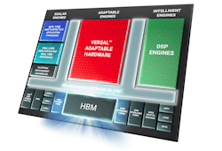
Xilinx’s Versal HBM FPGA packs in 32 GB of high bandwidth memory (Fig. 1). This platform adds HBM2e to the Versal Premium adaptive compute acceleration platform (ACAP) that includes dual-core Arm Cortex-A72 and dual-core Arm Cortex-R5F processors. The platform management controller provides overall system security and coordination. All of the major blocks are tied together by a programmable network-on-chip (NoC). The NoC provides faster bulk transfer compared to the configurable FPGA fabric in the Versal Adaptable Hardware.
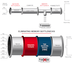
The HBM2e support provides 820 GB/s of bandwidth—eight times the bandwidth compared to a typical four-channel DDR5-6000 system with off-chip memory (Fig. 2). The HBM2e memory replaces 32 DDR5 memory chips while providing a faster, more power-efficient interface. It can reduce power requirements by 63% compared to off-chip DDR5.
Thanks to the higher bandwidth, Versal HBM can support more and faster network interfaces. On-chip accelerators like the crypto engine are designed to handle 400G networks in real time. The system also supports PCI Express (PCIe) Gen 5; its 1.5-Tb/s PCIe Gen 5 support is the basis for CXL and CCIX cache-coherent interfaces. The 112-Gb/s PAM4 interfaces can support 100 G/lane optics and 800 G infrastructures.
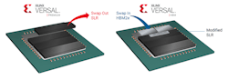
The Versal HBM FPGA is built on the same 2.5D interposer technology as Versal Premium (Fig. 3). The stacked silicon interposer (SSI) acts as a chip-based printed circuit board (PCB) that links multiple silicon die together. These are called super logic regions (SLRs). This technology, called chip-on-wafer-on-substrate (CoWoS) by TSMC, is the de facto standard for utilizing HBM2e memory.
There are significant advantages to using HBM2e memory, including a smaller footprint, higher bandwidth, lower latency, and lower power requirements. The top-end VH1782 comes with 32 GB of HBM2e memory and 752 Mb of SRAM. It has 5.6M system logic cells and 2.6M adaptable engines along with 10.9K DSP slices. Tools will be available in 2021 and silicon will be sampling in 2022.
About the Author

William G. Wong
Senior Content Director - Electronic Design and Microwaves & RF
I am Editor of Electronic Design focusing on embedded, software, and systems. As Senior Content Director, I also manage Microwaves & RF and I work with a great team of editors to provide engineers, programmers, developers and technical managers with interesting and useful articles and videos on a regular basis. Check out our free newsletters to see the latest content.
You can send press releases for new products for possible coverage on the website. I am also interested in receiving contributed articles for publishing on our website. Use our template and send to me along with a signed release form.
Check out my blog, AltEmbedded on Electronic Design, as well as his latest articles on this site that are listed below.
You can visit my social media via these links:
- AltEmbedded on Electronic Design
- Bill Wong on Facebook
- @AltEmbedded on Twitter
- Bill Wong on LinkedIn
I earned a Bachelor of Electrical Engineering at the Georgia Institute of Technology and a Masters in Computer Science from Rutgers University. I still do a bit of programming using everything from C and C++ to Rust and Ada/SPARK. I do a bit of PHP programming for Drupal websites. I have posted a few Drupal modules.
I still get a hand on software and electronic hardware. Some of this can be found on our Kit Close-Up video series. You can also see me on many of our TechXchange Talk videos. I am interested in a range of projects from robotics to artificial intelligence.
Comment About the Article
To join the conversation, and become an exclusive member of Electronic Design, create an account today!

Leaders relevant to this article: