Reap the Processing Power of FPGA-Integrated SDRs

Members can download this article in PDF format.
What you’ll learn:
- How FPGAs allow for the implementation of a reconfigurable SDR that’s scalable and can adapt to an unlimited number of transmission standards and techniques.
- How FPGAs are programmed.
- Important applications suitable for FPGAs, including those requiring high timing determinism as well as low latency.
Software-defined radio (SDR) is a highly flexible communication system that’s capable of configuring the hardware to perform various functions. An SDR’s components are implemented or defined in a programmable medium and provide a flexible link between hardware devices and the software interface.1
A field-programmable gate array (FPGA) is a semiconductor device based on a reconfigurable matrix of logic blocks. These devices, when integrated into a SDR, are incredibly powerful and can sustain high data throughput because such systems provide both the input/output bandwidth and the processing capabilities for implementing multi-gigasample sampling rates and gigahertz-range bandwidths.
This article discusses how FPGAs allow for the implementation of a reconfigurable SDR that’s scalable and can adapt to an unlimited number of transmission standards and techniques.2
FPGAs can be programmed to perform high-speed signal-processing tasks, enabling various characteristics of high-performance SDRs. This includes channelizing capabilities as well as processing (filters, decimation, interpolation, etc.) that allows for extremely fast downconversion/upconversion.
Furthermore, it enables modulation at an intermediate frequency (IF) before passing over JESD links to the digital-to-analog converter (DAC). The receiver side also can be programmed similarly for high-performance functionality. And reconfigurability means having extra resources to use additional IP cores or create custom digital signal processors (DSPs).
Also discussed in this article are the important applications suitable for FPGAs, including those requiring high timing determinism as well as low latency.
What are SDRs?
SDRs contain a radio front end (RFE) and a digital back end. The signals received from the antenna are fed directly to the RFE, where they’re modulated at an intermediate frequency (IF).
A SDR radio front end contains the receive (Rx) and transmit (Tx) functions to receive signals over wide tuning ranges. The digital back end, which is dedicated to performing various baseband processing tasks, is programmed onto reconfigurable hardware.
The front end of an SDR also can be implemented on a programming medium to make it more flexible and adaptable to a wide range of signals. For example, they can reduce the amount and complexity of components in a radar system because these components (waveform storage, pulse control systems, downconverting/upconverting, etc.) are programmed into a programming medium.
What is an FPGA?
An FPGA is a semiconductor/integrated hardware circuit that’s programmed to carry out multiple logical operations. Its architecture is centered around a matrix of configurable logic blocks (CLBs) with densities from 500 kLE to 10.2 MLE (LE=logic elements), and these blocks are reconfigurable into different logic gates and flip-flops by an engineer. Generally, CLBs consist of lookup tables (LUTs), multiplexers, and flip-flops, which are capable of implementing sophisticated logic functions.3
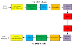
FPGAs have a reprogrammable, reconfigurable, and highly parallel computing fabric that’s able to handle very high throughput data rates. A current trend is to incorporate a hard-silicon processor core (such as the Intel Agilex HPS used with an Intel FPGA in Per Vices’ SDR products) within the FPGA die itself. This enables the processor to tackle routine, non-critical operations while the FPGA handles high-speed acceleration that’s beyond the processor’s capabilities. A simplified version of SDR processing in an FPGA is shown in Figure 1.
Similar to FPGAs, ASIC (application-specific integrated circuit) logic functions are specified using hardware description languages such as VHDL or Verilog, but they’re not reconfigurable. With ASICs, the resulting circuit is permanently etched into silicon. However, with FPGAs, the circuit is constructed by joining a number of reconfigurable logic blocks, i.e., CLBs. FPGAs are in between an ASIC, which performs highly specialized computational tasks very efficiently, and a CPU, which can execute any computational task.
Why Use FPGAs in SDRs?
The main reason for integrating FPGAs in SDRs is that latency can be controlled on the order of clock cycles. DSP functions such as digital downconverters (DDCs) and digital upconverters (DUCs) using coordinate rotation digital computer (CORDIC) algorithms, filtering, interpolation, decimation, etc., are done on FPGA devices incredibly quickly. Furthermore, sample buffers and the framing/de-framing of data of Ethernet packets also are performed on the FPGA.
The VITA Radio Transport (VRT) standard, also known as the VITA 49 protocol, is used to send the IQ data between the host system and the SDR via packetization of IQ data into the network protocol stack. An FPGA-based SDR platform is more reconfigurable and versatile than the other platforms available for the same task.
These high-performance devices can change waveforms or modulation schemes, for instance, flexibly by modifying software without the need to change the SDR platform. Hence, the most advanced implementation of SDR systems is based on the FPGA, as it provides a stable, reconfigurable, and reliable transceiver.
One major FPGA manufacturer within the industry is Xilinx (now part of AMD). FPGA manufacturers such as Xilinx generally ship a program/design tool for development on the FPGA. Xilinx uses software called Vivado to program and interface the with the FPGA and to implement complex algorithms, e.g., when designing an SDR’s digital backend system. Figure 2 shows the classical workflow from algorithm design to programming the FPGA.
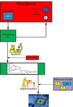
The following are the main steps in programming the FPGA:4
- Hardware architecture: Defining the circuitry by choosing and implementing suitable algorithms for the passband modulation, demodulation, signal generation, encoding, decoding, DDC, and DUC.
- Design: This step includes the development of hardware logic by utilizing the HDL (i.e., VHDL or Verilog) to write register transfer logic (RTL).
- Verification: Ensure the operation of the design is as per the requirements before programming the FPGA. The Verilog testbench or VHDL are common examples of the verification process. However, Universal Verification Methodology (UVM) is commonly used in commercial projects.
- Synthesis: The goals of register-to-register clock frequency are met by transforming the RTL into digital logic gates while using minimum FPGA resources.
- Implementation: Routing and programming of the targeted physical resource of the FPGA with its corresponding logic is performed in this step.
- Bitstream generation: This step synthesizes the network and generates a bitstream. To transform the HDL into a bitstream that programs the FPGA, a program called Vivado (Xilinx) or Quartus (Intel) is used (others are available).
- Debugging and lab test: The issues not identified in the verification step are debugged and test or real inputs are given to the programmed FPGA to evaluate its performance.
Important Applications Benefiting from FPGAs in SDRs
Already briefly discussed is the use of SDRs with FPGAs for radar applications. Similarly, wideband spectrum monitoring and recording is another one of the many applications that benefit from FPGA integration.
In spectrum monitoring, the targeted portion of the radio-frequency spectrum is monitored and the captured data is recorded and analyzed.5 When capturing a very large portion of the spectrum (i.e., wide bandwidth), multi-gigasample-per-second sampling is required as well as the ability to pass the data over 40- or 100-Gb/s Ethernet links to a host system where it can be processed.
To do that, we need to have extremely fast ways of communicating between the ADC and FPGA, using JESD links. The JESD204B protocol is employed for transferring the data to the FPGAs when the high-speed ADCs fall into the range of gigasamples-per-second. This protocol has standard layered specifications, and assigned tasks are performed by the individual layers in the specification. The tasks of the individual layers in the JESD204B protocol are as follows:6
- Application layer: Allows JESD203B link to map data and configure.
- Transport layer: Reduces the EMI effects by spectral peak spread via mapping of conversion samples to and from the framed non-scrambled octet.
- Data link layer: 10-bit character encoding is performed for the scrambled octets.
- Physical layer: Operation of transmitting and receiving the characters at line-rate speeds. The serializer/deserializer (SerDes) layer includes the data recovery, clock, receivers, drivers, and serializers.
FPGAs provide computationally intensive features and are much more powerful than standard CPUs when performing processing in real-time. They’re low-latency devices due to the hardware’s parallel architecture and deterministic nature, making them ideal for low-latency links. However, any DSP does take time to execute, which must be considered while designing low-latency communication links with SDR.
Latency can be reduced on the FPGA by using a modified stock image that has a low-latency IP core and a small sample buffer size. Moreover, FPGAs play a key role in applications such as those involving low-latency distributed networks and high-frequency trading, where a millisecond of latency can mean multimillion-dollar profits or losses. They’re also useful for collecting market data associated with round-trip latency used by HFT firms.
In addition, SDRs with FPGAs can be used to build custom modems into them that work at extremely fast rates. For instance, research is being conducted on CORDIC-based digital demodulation in radar systems.
In one case, a first-order complex digital phase-locked loop (DPLL) for an I/Q channel radar demodulator using a pipelined CORDIC architecture was designed.7 The CORDIC offers the opportunity to calculate the desired trigonometric computation simply and efficiently. In another example, 5G modem technologies also benefit from FPGAs in their SDRs in remote radio heads.8
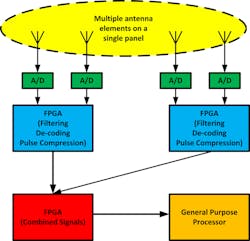
Computationally intensive applications such as active electronic-scanned-array (AESA) radar also benefit from FPGAs. For instance, adaptive beamsteering/forming technologies take advantage of FPGA channelization for antenna arrays used in AESA radar applications.9 The frequency-domain beamforming architecture is utilized by the signal-processing structure. Figure 3 shows the basic structure of a SDR with FPGA for beamforming/steering.
SDRs with FPGA capabilities allow for easier implementation of advanced signal-processing algorithms, as well as provide firmware that can be updated and reconfigured as per the requirements of the user application. FPGAs facilitate integration with other systems by enabling the user to develop a custom communication interface or using the latest radio protocols.
The same SDR transceiver can be interfaced to work with other products or systems simply by upgrading FPGA cores and/or updating software. This includes the ability of one SDR transceiver to work with any new GPS/GNSS constellation, work with various types of modulation schemes in different bands and tuning frequencies, or even have SDRs seamlessly integrate into legacy systems.
FPGAs are constantly scaling in the number of CLBs and gates—and thus design complexity—as open-source HDL cores are provided by a community of amateurs and professionals who share the demanding workload, documentation, and extensive verification.
Historically, IP cores are proprietary and require expensive licensing, which can hinder researchers or startups due to cost constraints. However, HDL IP cores for FPGAs are now readily available. There are various open-source HDL libraries for implementing FPGAs, allowing for greater functionality and capabilities without extensive development time.
Many open-source FPGA cores beneficial to SDRs are available, too, from IIR/FIR filters to oscillators to IQ-pair phase and gain correction codes. Intel and Xilinx also offer their own optimized HDL IP cores as a library. Of course, if there’s no IP core available for your SDR application and you want to design one from scratch, SDR manufacturers have lots of resources accessible to users for custom design.
Conclusion
While many SDRs exist on the market, those with FPGA resources are needed in the most demanding and high-performance RF applications. In this article, we defined FPGAs, how they’re programmed, and the importance of them in SDR receive/transmit functionality. We also discussed the benefits they bring to numerous applications, including spectrum monitoring, low-latency links, distributed networking, AESA radars, and 5G base-station technologies.
As RF system capabilities evolve and extend in accordance with the new market requirements, SDRs with FPGAs can be used for all aspects, ranging from algorithm development to simulation to full production systems.
References
1. X. Cai, M. Zhou, and X. Huang, “Model-Based Design for Software Defined Radio on an FPGA,” IEEE Access, vol. 5, pp. 8276–8283, 2017, doi: 10.1109/ACCESS.2017.2692764.
2. D. F. Macedo, D. Guedes, L. F. M. Vieira, M. A. M. Vieira, and M. Nogueira, “Programmable Networks—From Software-Defined Radio to Software-Defined Networking,” IEEE Communications Surveys & Tutorials, vol. 17, no. 2, pp. 1102–1125, 2015, doi: 10.1109/COMST.2015.2402617.
3. R. Singh, “FPGA Vs ASIC: Differences Between Them And Which One To Use?,” 2018. https://numato.com/blog/differences-between-fpga-and-asics/ (accessed Apr. 16, 2022).
4. https://www.mathworks.com/discovery/fpga-programming.html.
5. https://www.everythingrf.com/community/software-defined-radio-use-case-for-spectrum-monitoring.
6. https://www.analog.com/en/technical-articles/understanding-layers-in-jesd204b-specification.html.
7. Mandal, Amritakar, and Rajesh Mishra. "FPGA implementation of pipelined CORDIC for digital demodulation in FMCW radar." Infocommunications J 5, no. 2 (2013): 17-23.
9. https://www.curtisswrightds.com/news/articles/beamforming-fpgas-rise-to-the-challenge.html.
About the Author
Brendon McHugh
Field Applications Engineer, Per Vices Corp.
Brendon McHugh has a degree in theoretical and mathematical physics from the University of Toronto and works at Per Vices as a Field Applications Engineer and Technical Writer.
Comment About the Article
To join the conversation, and become an exclusive member of Electronic Design, create an account today!

Leaders relevant to this article: