3D NAND Flash Memory Stacked High at Micron
Check out more coverage of the 2022 Flash Memory Summit.
Micron has started mass production of its most advanced triple-level-cell (TLC) 3D NAND chips made up of 232 layers of memory cells, pulling ahead in the race to dominate the skyline in the flash-memory market.
The U.S. memory chip giant said the chips deliver as much as double the density of bits stored than other TLC NAND devices on the market, packing in 14.6 Gb for every square millimeter. The chips support about 40% more density than its 176-layer 3D NAND released in 2020, promising higher capacities and faster speeds that will pay dividends in everything from smartphones to data centers and the intelligent edge.
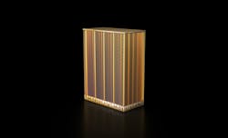
These improvements translate to 1 TB of storage capacity in a single die, according to Micron. The company can bundle 16 of the dies in a package 3X smaller than a postage stamp that can store 2 TB.
The improved density means the 3D NAND flash chips fit into packages measuring 11.5 × 13.5 mm, which is about 28% smaller than its predecessor, saving circuit-board space in solid-state-drive (SSD) and embedded NAND solutions.
Micron is already shipping the new NAND flash in its consumer Crucial SSDs and as components to OEMs. While the company is the market leader when it comes to layer count, its competitors are close behind.
Samsung plans to roll out 3D NAND chips with more than 200 layers of memory cells by the end of 2022, or early next year at the latest, and ramp up mass production of the memory chips by the first half of 2023.
At SK Hynix, the plan is to start mass production of its most advanced 3D NAND flash, which features up to 238 layers for use in PCs, smartphones, and data centers, also by the first half of 2023. It is currently shipping sample quantities of the 238-layer 3D NAND.
Silicon High-Rise
Micron said the new 232-layer 3D NAND leverages many of the same innovations in previous generations, including a new generation of its CMOS-under-Array (CuA) technology.
This places a layer of CMOS logic on the ground floor of the 3D NAND stack. The logic is used to coordinate all of the read and write operations and moves data into and out of the memory cells as fast and efficiently as possible. Improvements to the logic increase the data-transfer rate of the new memory chips to 2.4 GB/s on the Open NAND Flash Interface (ONFI) bus, which is 50% faster than its previous generation.
At 2.4 GB/s, the 232-layer 3D NAND meets the low-latency and high-throughput demands of workloads such as artificial intelligence (AI) and machine learning, real-time analytics, and cloud computing.
Stacked on top of the logic are the layers of memory cells. More floors of NAND flash stacked on top of each other means more bits can be stored per square millimeter, driving up the density and reducing costs.
Micron is taking advantage of the same replacement-gate (RG) technology as its 176-layer 3D NAND, which reduces the capacitance between memory cells and, thus, improves performance, power, and endurance.
Unlike other types of memory, 3D NAND resembles a silicon high-rise where ultra-thin layers of memory are stacked in three dimensions with short vertical connections between them that act like elevator shafts.
The memory cells themselves resemble tiny cylinders embedded in silicon. They start out as relatively deep holes—also called channels—drilled from the top to the bottom of the memory cell. The walls of the hole are coated with advanced materials before what’s left is filled to form the part of the cell that stores data.
The memory cells in 3D NAND are stacked vertically, so a problem in a single cell can hurt the performance of the entire string. The challenge is physically stacking more floors of flash memory on top of each other while keeping the channels in perfect alignment.
Instead of stacking all 232 floors of memory on top of each other, Micron uses a "dual-stack" architecture, where a pair of 116-layer dies are sandwiched together in a process called string stacking.
Bandwidth Boost
Micron said it is pairing the improved storage capacity with a major leap in performance. That’s largely due to its new six-plane architecture, giving it the most planes per die of any TLC 3D NAND flash on the market.
A plane is a region inside a flash-memory chip that can respond to I/O requests independently—sort of the same way the cores in a CPU can run several computations in parallel. In general, more planes mean the 3D NAND memory can carry out more read and write commands at the same time, thus increasing performance.
The additional memory planes, coupled with its 50% increase in memory bandwidth, results in what Micron said is 100% higher write bandwidth and 75% higher read bandwidth than its prior generation of 3D NAND. They reduce I/O collisions on internal paths, in the same way a highway with more lanes help to lessen congestion and more efficient traffic flows. The result is improvements in latency.
According to the company, the 256-layer 3D NAND is also the first in production to support the NV-LPDDR4 interface that uses lower voltages to reduce the power use per bit by more than 30% compared to its predecessor. The I/O interface is backward-compatible to support legacy memory controllers.
Micron is still in the early stages of its mass production but plans to ramp up volumes through 2022.
Check out more coverage of the 2022 Flash Memory Summit.
About the Author

James Morra
Senior Editor
James Morra is the senior editor for Electronic Design, covering the semiconductor industry and new technology trends, with a focus on power electronics and power management. He also reports on the business behind electrical engineering, including the electronics supply chain. He joined Electronic Design in 2015 and is based in Chicago, Illinois.
Comment About the Article
To join the conversation, and become an exclusive member of Electronic Design, create an account today!

Leaders relevant to this article: