Plotting Out a Path to the Trillion Transistor Era

Check out our coverage of the Hot Chips 2022 event.
Intel CEO Pat Gelsinger said that it will take more than smaller, cheaper transistors to propel Moore’s Law in the coming years.
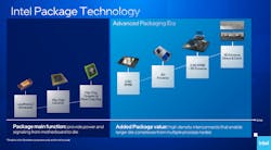
The Santa Clara, California-based company used the keynote of the annual Hot Chips conference to preview how it sees the world of semiconductors shaking out in the next several years. Gelsinger said it is entering a new era that will require a shift from its relentless pursuit of trying to fit everything on a single system-on-chip (SoC) à la Moore’s Law. Instead, Intel will focus on what it can squeeze in a system-in-package (SiP).
Everything from its future flagship Sapphire Rapids Xeon Scalable CPUs for the data center to its new family of personal-computer chips, called Meteor Lake, are enlisting 2.5D and 3D tile-based chip designs to wring out more performance, he said.
The new philosophy is taking shape as Intel looks to return to the top of its game after falling behind in the high stakes battle to build the most advanced chips. Intel’s struggles are putting its dominance in data centers and other markets in peril for the first time in many years. Gelsinger is trying to execute on one of the company’s most ambitious roadmaps in quite some time to overtake TSMC and other rivals that have pulled ahead.
He is also building up a business called Intel Foundry Services to take on TSMC. It manufactures chips on contract according to others’ designs, while relying on rival foundries to make more of its own products.
He said the concept of a foundry is becoming more complicated than ever. Foundries now have to be in the business of producing not only wafers, but whole systems tied together with software.
"If you think about it, the rack is becoming a system,” said Gelsinger. “And the system is becoming an advanced package of multiple dies and chiplets. Literally, the system is becoming the advanced packaging technology of the future.”
Intel’s role as a “systems foundry” is to help expand the ecosystem around chiplets and 2.5D and 3D advanced packaging technologies, creating new possibilities for innovative custom chips and system-level integration.
From Chip to Package
The remarks signal that Intel’s CEO does not believe in the impending demise of Moore’s Law, even as manufacturing chips becomes more costly and technically challenging.
"Moore's Law—this continuing doubling of transistor capability as the dimensions shrink over time—is fundamentally the driver of everything that we’ve been able to accomplish," said Gelsinger.

But this gives it new ways to make chips more cheaply, more adaptable to its customers’ software, and able to meet the demands for more compute, connectivity, and AI in everything that runs on semiconductors.
While Intel can squeeze more than 100 billion transistors in a package today, he said the U.S. chip giant has process and packaging technologies in the pipeline that will allow it to hit 1 trillion by the end of the decade.
He cited innovations in transistor design, including its upcoming gate-all-around (GAA) transistors called RibbonFETs and new Power Via backside power-delivery system, coupled with the use of extreme-ultraviolet (EUV) technology and High-NA EUV later on. These are the keys to building smaller, faster, and more power-efficient transistors in the coming years, he said.
But innovations in transistor design will only take it so far. Intel is also tapping into its wide range of 2.5D packaging, including embedded multi-die interface bridge (EMIB), and its 3D logic-stacking technologies to help tie more silicon die—and thus, transistors—together in high-density chip packaging.
A stark example of this trend is the high-performance GPU being built by Intel for the U.S. Aurora supercomputer. The processor is composed of close to 50 active silicon tiles connected with a combination of Intel’s 2.5D and 3D packaging.
Each tile in the package, which packs 3,100 square millimeters of silicon into a 2,330-mm2 footprint, was made using different technology nodes both from Intel and TSMC, translating to over 100 billion transistors.
Gelsinger pointed out that “the system problems of today will become the chiplet problems of tomorrow.”
New Philosophy
What it hopes to do is give its customers the same ability to disassemble chips that could be constrained by die area, cost, or power and then reassemble the chiplets into a package.
The concept behind chiplets—or tiles as Intel calls them—is divide and conquer. These tiny squares of silicon are sliced out of what would previously have been a single monolithic slab of silicon. The chiplets are then reassembled in a package that is more than the sum of its parts. In addition to saving space, this gives designers the freedom to glue together a wide variety of chiplets, as if assembling parts on a very small circuit board.
Monolithic dies—in leading-edge server processors such as Intel’s—are hindered by other weaknesses. They have more room for imperfections that hurt yields, making them more expensive per transistor at smaller nodes.
What Gelsinger also noted is that all of the different tiles in a package can be manufactured separately using whatever process node is most appropriate for different functions: power, RF, analog, advanced logic.
That way, the most advanced process technologies can be used where it counts—in the main compute tiles. Building non-critical tiles on legacy nodes—or even reusing tiles from preexisting chips—saves resources compared to designing new IP blocks. He called this approach applying "the right transistor for the right problems.”
“But we also will need to tie these together in a very easy-to-use composable fashion that gives the designers the abstractions that enable them to do more complex things without the detail of each execution and hardened IP at the chip level.”
Gelsinger is building up Intel’s foundry business to be open to everyone, giving its customers access to libraries of IP, both from its internal repository and from outside firms, in addition to software. He said Intel is willing to roll out chips based on instruction set architectures (ISAs) from x86, Arm, to RISC-V. It will also use foundry offerings, such as its Chiplet Studio Suite of technologies, to help the chiplet ecosystem mature.
Connective Tissue
Key to all of this will be creating a standard interface that will allow everything to fit together seamlessly.
To that end, Intel has been one of the driving forces behind the emerging “Universal Chiplet Interconnect Express” (UCIe) interface as an open, industry-standard die-to-die interconnect built on top of the PCIe bus.
What makes the UCIe standard stand out is that many of world’s top semiconductor firms are getting behind it, with AMD, Arm, Marvell, NVIDIA, and Qualcomm, plus foundries Samsung and TSMC, teaming up with Intel.
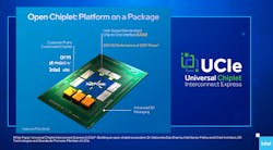
Also backing UCIe are cloud and technology leaders Google, Meta, and Microsoft. Around 50 companies in all have joined the UCIe Consortium to help build a chiplet ecosystem, opening the door for mixing and matching of IP designed and manufactured on varying process technologies by different vendors in a package.
“Now we’re taking a monolithic system on a chip that could be constrained in die size, cost, and power, and being able to disaggregate it onto a solution that takes advantage of not only the advanced packaging, but all the standard mix-and-match capabilities that the open UCIe standard can enable,” said Gelsinger.
As more companies adopt 2.5D and 3D chip designs, a plug-and-play interface like UCIe should also help reduce cost through economies of scale and ease of integration, making the approach more accessible.
“You may say, ‘I’m getting one of the chiplets from Intel, and I’m getting one of the chiplets coming from a TSMC factory,’” he said. “Maybe the power-supply components are coming from TI, maybe there is an I/O component coming from GlobalFoundries. Intel has the best packaging technology, so they would be the one assembling all those chiplets together into the marketplace, but maybe it is another provider as well.”
Gelsinger added, “We do see the mix and match. And when I say the rack is becoming a system, the system is becoming an advanced chiplet based on a package, that’s exactly what we mean, how we see it evolving.”
Read more articles from our coverage of the Hot Chips 2022 event.
About the Author

James Morra
Senior Editor
James Morra is the senior editor for Electronic Design, covering the semiconductor industry and new technology trends, with a focus on power electronics and power management. He also reports on the business behind electrical engineering, including the electronics supply chain. He joined Electronic Design in 2015 and is based in Chicago, Illinois.
Comment About the Article
To join the conversation, and become an exclusive member of Electronic Design, create an account today!

Leaders relevant to this article: